β: This English translation is in beta — the Traditional-Chinese original is the authoritative version.
Lab 32 — MOS Level-1 Equation-Level Ring: Extracting the ISF from Transistor Equations
Breadcrumb: Simulation labs › System & advanced › This page (MOS Level-1 equation-level ring ISF). Upstream: lab_03 (toy triangular ISF), lab_04 (impulse extraction method); related: waveform_slope, real_oscillator_topologies.
Every ring ISF on this site so far has been a hand-placed shape: the triangle in lab_03 was only a sketch of "energy concentrated in the transitions" — its height, width, and sign were never computed. This page takes an honest step forward: model each inverter stage with the MOS Level-1 (Shichman-Hodges) square-law equations — cutoff/triode/saturation, real , , , — integrate the steady-state oscillation in numpy with a fixed small step, then assume nothing and directly measure node 1's phase by phase with the impulse method of [P1].
Model-level statement (applies to the whole page): this lab is MOS Level-1 equation-level (Shichman-Hodges), not SPICE/BSIM/PDK. It is one level more honest than a toy model (the currents really come from device equations, and the ISF really is measured), but it is still not transistor-level sign-off: no velocity saturation, no subthreshold, no parasitic RC, and no noise sources (see Section 11). ngspice is not installed in this environment — this is precisely a demonstration of the upper limit of "how honest you can be without SPICE."
Physical intuition (conclusion first): a ring node only fears a kick while it (or the gate driving it) is switching. When pinned to a rail, the low output impedance of the driving stage swallows the injected charge within tens of ps () and no phase trace remains; during a transition, directly shifts the edge in time, and that shift propagates permanently. So the measured is dual-lobe: a positive lobe around the rising edge (advance) and a negative lobe around the falling edge (delay) — exactly the signature of [P2] Fig. 5/Fig. 6 (p.793).
Three rungs on the model ladder; this page stands on the middle one:
| Level | Where the current comes from | Where the ISF comes from | Site counterpart |
|---|---|---|---|
| toy model | no current, waveform drawn directly | hand-placed shape (, triangle) | lab_02, lab_03 |
| equation-level (this page) | Level-1 square-law device equations | measured with the impulse method | lab_32 |
| SPICE + PDK | BSIM4/PSP + extracted parasitics | measured via transient/PSS+adjoint | not on this site (honesty note) |
The SPICE/PDK rung would further add: velocity saturation and mobility degradation (short-channel no longer ), subthreshold conduction (exponential tail when is below ), channel-length modulation (), gate capacitances (Miller coupling), layout parasitic RC, corners/mismatch, and the noise models (thermal + flicker). All of these change the numbers, but they do not change the mechanism this page teaches: the ISF is a physical quantity that can be measured directly from device equations.
1. Teaching goals
- Write the MOS Level-1 (Shichman-Hodges) three-region IV equations as integrable node equations and integrate the 3-stage ring to a steady-state oscillation ( GHz, measured, not computed by formula).
- Extract node 1's with the impulse method of [P1]: 24 injection phases, fC, wait periods, then read the permanent phase shift by threshold-crossing time comparison.
- Verify the [P2] signatures: dual-lobe shape, energy concentrated near the node's own transitions, sensitivity approaching 0 while pinned to the rails.
- Compare against the triangular approximation of [P2] Fig. 6 (p.793) and the of Eq.(16) (p.794) — which parts hold, and which distort at .
- Honest scoping: this level extracts only the deterministic ISF; getting to phase noise still requires noise sources ([P1] Eq.(21), see device_noise_mapping).
2. Mathematical model
2.1 Device: MOS Level-1 (Shichman-Hodges) square law
NMOS (, ):
The PMOS is the exact mirror (replace with ).
- Unit check: (), dimensionless, ✓.
- Parameters chosen for a symmetric inverter: equals , V, V — rise/fall symmetric, so we expect ([P1] symmetry argument; the measurement gives , see Section 9).
- This is exactly SPICE's "Level 1" model (external literature, not among the five source PDFs): H. Shichman and D. A. Hodges, "Modeling and simulation of insulated-gate field-effect transistor switching circuits," IEEE J. Solid-State Circuits, vol. 3, no. 3, pp. 285–289, Sep. 1968.
- In code the three regions are implemented as a single clamped expression: , , — pointwise equal to the piecewise definition above (substitute for cutoff and for saturation). If an injection pushes a node above , the code swaps source/drain to handle reverse conduction and stays physical.
2.2 Circuit: node equations of a 3-stage single-ended inverter ring
Stage takes node (mod 3) as input, drives node , each node loaded by :
- Unit check: ✓.
- Integration: fixed-step forward Euler, fs. The fastest node time constant is ps, , huge stability margin; halving changes by only (relative, verified by rerun).
- An odd-stage single-ended inverter ring has no stable DC point; integrating from an asymmetric initial condition (0.9, 0.1, 0.5 V) for 11 ns reaches the steady-state limit cycle; the measured period spread is only of order ps (deterministic, no noise sources).
2.3 ISF extraction: impulse injection + threshold-crossing comparison
Inject fC into node 1 at phase ; the equivalent voltage step ([P1] Eq.(9), p.182):
Wait periods (the amplitude deviation has long been dissipated by the driving stage, leaving only the phase shift), then compare the perturbed run against an unperturbed run using the same integrator and the same initial condition: read the times at which node 1's rising edge crosses , fold the time difference back into , and convert:
This is exactly the operational definition of [P1] Eq.(10)–(11) (p.182) (the same thing lab_04 did on a sinusoidal oscillator, now on an equation-level circuit). Numerical feel (using the measured peak): , ⇒ rad; ps — a 0.9% permanent shift of the ps period, well within the resolution of threshold crossing with linear interpolation.
- Unit check: ✓; dimensionless ✓.
- Linearity premise ([P1] Fig. 6, p.182): halving changes by only 0.1% (1.1284 vs 1.1295, verified by rerun), confirming small-signal linear operation.
- The injection instant is quantized to fs, a phase error , negligible.
3. Block diagram
4. Core Python code
Excerpt from simulations/lab_32_mos_level1_ring.py (checked against the source). Device
three-region single expression, ring derivative, and the extraction main loop:
def _sq_v(vgs, vds, beta, vt):
    """Level-1 square law (vds>=0): cutoff/triode/saturation in one clamped expression."""
    vov = np.maximum(vgs - vt, 0.0)      # cutoff -> vov = 0
    vde = np.minimum(vds, vov)           # saturation -> vde = vov
    return beta * (vov - 0.5 * vde) * vde

def ring_dvdt_v(v):
    """dV/dt [V/s]; v shape (..., 3), stage-i input = node i-1 (np.roll)."""
    vin = np.roll(v, 1, axis=-1)
    i_n = (_sq_v(vin, np.maximum(v, 0.0), BETA_N, VTN)
           - _sq_v(vin - v, np.maximum(-v, 0.0), BETA_N, VTN))      # reverse-conduction term
    i_p = (_sq_v(VDD - vin, np.maximum(VDD - v, 0.0), BETA_P, VTP_ABS)
           - _sq_v(v - vin, np.maximum(v - VDD, 0.0), BETA_P, VTP_ABS))
    return (i_p - i_n) / CL

# 26 rings run in lockstep: run 0 = unperturbed reference, runs 1..24 = the 24 phases, run 25 = linearity check
for k in range(n):
    r = inj.get(k)
    if r is not None:
        V[r + 1, 0] += DV                # dV = dq/CL ([P1] Eq.(9))
    V += dt * ring_dvdt_v(V)             # fixed small-step Euler
    rec[k + 1] = V[:, 0]                 # record node 1 for threshold-crossing comparison

tc = first_after(rising_crossings(x[:, r], dt), t_late)   # after >= 20 periods
dts = (tc - tc_ref + 0.5 * T) % T - 0.5 * T               # fold back into [-T/2, T/2)
gamma = -w0 * dts * QMAX / DQ                             # Δφ·q_max/Δq
The reference run and the perturbed runs share the same integrator and initial condition, so Euler's (first-order) period bias cancels exactly — the same differential-measurement trick used in the numerical verification of derivation_floquet_ppv (lab_25).
5. Full script path
simulations/lab_32_mos_level1_ring.py
(depends on compute_fourier_coefficients, gamma_rms, and
gamma_triangular from simulations/common/isf_utils.py; savefig from
simulations/common/plot_utils.py.)
Run with: PYTHONPATH=. python simulations/lab_32_mos_level1_ring.py (about 10 s on a single
machine, no randomness, fully reproducible).
6. Parameter table
| Parameter | Code variable | Value | Meaning |
|---|---|---|---|
| Supply | VDD | 1.0 V | supply |
| NMOS threshold | VTN | 0.4 V | |
| PMOS threshold | VTP_ABS | 0.4 V | ( V) |
| NMOS process constant | KPN | ||
| PMOS process constant | KPP | ||
| Size ratios | WLN / WLP | 2 / 4 | , (compensates ) |
| Effective strength | BETA_N = BETA_P | symmetric inverter ⇒ | |
| Node load | CL | 10 fF | lumped capacitance per node |
| Stage count | N_STAGES | 3 | single-ended inverter ring |
| Integration step | DT | 25 fs | |
| Injected charge | DQ | 0.5 fC | V |
| Maximum charge | QMAX | 10 fC | |
| Injection phases | N_PHASES | 24 | one point every |
| Wait time | — | 22 | measure only periods after injection |
7. Unit table
| Quantity | Symbol | Unit | Notes |
|---|---|---|---|
| Node voltage | V | 0 to (measured 0.0038–0.9962 V) | |
| Drain current | A | Level-1, three regions | |
| Process constant | A/V² | ||
| Period / frequency | / | s / Hz | 816.186 ps / 1.2252 GHz |
| Stage delay | s | ps ([P2] Eq.(15)) | |
| Injected charge | C | 0.5 fC | |
| Phase shift | rad | ||
| ISF | dimensionless | measured, not assumed | |
| Fourier coefficients | dimensionless | [P1] Eq.(12) |
8. Simulation figure
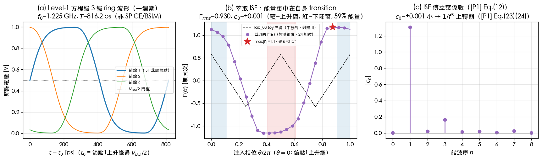
9. How to read the figure
(a) Waveforms (one period): the three nodes toggle in turn, spaced ps apart (a 3-stage ring has 3 edges per half period). GHz and ps are measured; inverting [P2] Eq.(15) gives a per-stage delay ps. Note that at the waveform is far from square — each transition's 10%–90% window occupies roughly a fifth of the period, and the flat tops on the rails are not actually long.
(b) Extracted (the star of this page): the 24 purple dots are 24 independent impulse experiments. The structure they read out:
- Dual-lobe, correctly registered: the positive lobe sits around node 1's own rising edge (, ), the negative lobe around its own falling edge (, ). Positive charge advances the phase at the rising edge and delays it at the falling edge — the signs are not postulated, they are measured.
- Peak at the onset of a transition: occurs at , i.e. before the rising edge; the deepest point of the negative lobe, , is at , i.e. before the falling edge — mirror symmetric. The physics: the driving gate (node 3) is starting to flip and the transistor holding the rail is letting go; charge injected at that moment is neither swallowed nor wasted — it directly shifts the imminent edge. That hurts the most.
- Energy concentrated in the transitions: the 10%–90% transition windows (shaded) take 40.7% of the period yet contain 58.7% of the energy. At the concentration looks "not dramatic enough," and the honest reason is: one stage switches every , and each transition takes — the ring has almost no quiet moment; the quietest phases ( zero crossings) are at (). The [P2] picture is: as grows, the transition fraction shrinks, the lobes narrow, and the quiet zones widen — a single- lab like this one can only demonstrate the mechanism, not verify the scaling (see below).
- Against the lab_03 toy triangle (black dashed): the toy guessed the right direction ("concentrated in the transitions"), but (i) its peak height is half the measured ; (ii) the toy puts a positive peak on both edges, while the measurement gives one positive, one negative; (iii) at the measured lobes are wide flat-tops, not sharp triangles. That is the gap between a hand-placed shape and a measured one.
- Against from waveform_slope: inside a lobe, corresponds to V/s, consistent with the waveform slope; but on the rails the slope goes to 0 while also goes to 0 — because the inverse-proportionality assumes the perturbation stays on the orbit, whereas on the rail the driving stage is a low-impedance termination that simply swallows the charge. The two pages are complementary, not contradictory.
(c) stems: dominates, is second, and the even harmonics are nearly 0 — a wide flat-top, odd-symmetric dual lobe is naturally dominated by odd harmonics. The most important stem is the one you can barely see: . Because rise/fall were designed symmetric via , flicker upconversion (, [P1] Eq.(23)(24), ) would be suppressed to almost nothing — if a flicker source had been modeled (this lab has none, see Section 11). Parseval ([P1] Eq.(20)): vs , consistent.
Three measurement-quality checks (printed by the actual run): halving moves by only ; halving moves by only 0.1%; period spread ps. The numbers are trustworthy.
10. Mapping to paper equations/figures
- Operational ISF definition: [P1] Eq.(10)–(11), p.182 together with (Eq.(9), p.182) — this lab's extraction procedure uses these two equations as the measurement instrument.
- Linearity premise: [P1] Fig. 6, p.182 ( for small charge; this lab verifies by halving , 0.1% difference).
- Ring ISF shape: [P2] Fig. 5, p.793 (simulation-extracted ring ISF, energy concentrated in the transitions), Fig. 6, p.793 (approximate waveform + triangular ISF approximation). This lab's measurement: dual lobes, peaks at the transition onsets ✓; but the lobes are wide flat-tops rather than narrow triangles — the triangular approximation only becomes accurate at large (small transition fraction).
- Frequency: [P2] Eq.(15), p.794: ; this lab back-solves ps.
- : the correct reading of [P2] Eq.(16), p.794 is that the square root covers only the constant: (at this is , the solid line in [P2] Fig.8). Plugging in : gives , the anchor gives . The measured is 88% above the reference and 22% above the anchor — same order of magnitude, but no single lines up exactly ( was not fitted to this circuit, and at the triode/saturation mix and the symmetric inverter's actual waveform naturally deviate from the triangular/exponential approximation used in the paper's derivation). A single cannot verify the scaling — it can only serve as a ballpark magnitude check; verifying the scaling requires sweeping (this script's vectorized derivative supports any stage count; the sweep is left as an extension exercise).
- Next step toward phase noise (not done in this lab): plugging the measured and into [P1] Eq.(21) () and Eq.(23)(24) () still requires the device noise PSD and cyclostationary weighting (effective_isf).
11. Limitations and approximations — where this level of honesty ends
What we see beyond the toy model: , the waveforms, and the shape/sign/magnitude of are all measured from device equations; symmetric design ⇒ can be engineered, not merely declared.
What remains invisible (needs SPICE/BSIM/PDK or more modeling):
- Level-1 physics gaps: no velocity saturation/mobility degradation (in advanced nodes rather than , which changes transition slopes and lobe shapes); no subthreshold conduction (real devices still carry an exponential tail current for below , softening the lobe edges); (no channel-length modulation).
- Lumped only: no (Miller coupling would make edges tug at each other), no layout parasitic RC. fC uses the nominal value (measured swing 99.2% of , 0.8% off).
- No noise model at all: this lab is deterministic — it extracts the ISF itself and produces no phase noise. Thermal () and flicker sources, and their cyclostationary modulation, are not at this level.
- Single , single corner: does not verify , does not look at PVT.
- Numerics: fixed-step first-order Euler (convergence measured at ); injection-phase quantization ; threshold crossing via linear interpolation.
Key takeaways
- MOS Level-1 (Shichman-Hodges) equation-level 3-stage ring: GHz, ps, ps ([P2] Eq.(15)) — not SPICE/BSIM/PDK.
- The impulse method ( fC, 24 phases, wait periods, threshold-crossing comparison) measures a dual-lobe ISF: positive lobe around the rising edge (), negative lobe around the falling edge (), peak at before the rising edge.
- The [P2] signatures hold: 58.7% of the energy inside the 40.7% transition windows; at the lobes are wide flat-tops, and the triangular approximation ([P2] Fig. 6) only becomes accurate at large .
- ([P2] Eq.(16), scaling: gives 0.4937, the anchor gives 0.760 — same order of magnitude, ballpark only; not fitted, single does not verify the scaling); comes from the symmetric design ⇒ weak upconversion ([P1] Eq.(23)(24)).
- This level extracts the ISF itself; reaching phase noise still requires noise sources and cyclostationary weighting.
Further reading
- lab_03 — ring toy model: where the hand-placed triangular ISF that this page replaces came from.
- lab_04 — impulse extraction method: the same measurement instrument's first appearance, on a sinusoidal oscillator.
- waveform_slope — waveform slope and sensitivity: why inside a lobe and why it fails on the rails.
- real_oscillator_topologies — real topologies: where the ISF of cross-coupled LC / Colpitts / CMOS ring stages comes from.
- device_noise_mapping: fills in the step this page deliberately skipped — device noise PSD × ISF → phase noise.