β: This English translation is in beta — the Traditional-Chinese original is the authoritative version.
Waveform Symmetry and Flicker Upconversion
Prerequisites: flicker_noise_upconversion (the full flicker → derivation; this page is its design-facing counterpart), fourier_series_of_isf (the ISF's Fourier coefficients and Parseval), device_noise_mapping (the of the effective ISF is the real culprit) | Next: waveform_slope, serdes_clocking_connection
This page answers a question that must be settled at the layout/topology stage: why does a waveform with symmetric rise/fall have noticeably lower close-in (near-carrier) 1/f³ phase noise? The answer is hidden entirely in one Fourier coefficient of the ISF — the DC term .
Physical intuition (conclusion first): a device's flicker noise (1/f noise, slow-varying noise in the gate/channel) is a near-DC, low-frequency noise. Low-frequency noise should not normally contaminate a high-frequency carrier — but the ISF is a periodic function, and its DC component acts like a "rectifier": it accumulates low-frequency device noise with a persistent sign into the phase, upconverting it to a close-in 1/f³ skirt near the carrier. If the rise/fall is perfectly symmetric, the ISF's positive and negative areas cancel over one period, , and this upconversion channel is shut off.
Step 1: why only upconverts flicker
Write the ISF as a Fourier series ([P1] Eq.(12), p.183):
Substitute into the LTV phase response ([P1] Eq.(13), p.183), splitting the phase into contributions from each harmonic:
- Key observation: device flicker-noise energy is concentrated near DC (). In the expression above, every term () carries a factor, which multiplies the low-frequency noise by a high-frequency carrier — a mixing operation that moves the noise to near , away from DC.
- Only the term has no carrier: it performs a pure integration of the low-frequency noise. Low-frequency noise stays nearly the same sign over an extended interval, so the integral accumulates without cancelling, continuously driving the close-in phase → upconverted into 1/f³.
- In one line: acts like a mixer (it moves the noise away), while acts like an integrator (it retains and amplifies DC noise).
Step 2: 1/f³ phase noise and the corner formula
Feed the device flicker model ([P1] Eq.(22), p.185)
into the phase noise from the -only channel to get the 1/f³ region ([P1] Eq.(23), p.185):
- Slope dimension check: (from the phase integration) times (from flicker's factor) = → dB per decade, exactly 1/f³. ✓
- Key point: the numerator is . A symmetric waveform drives → the entire 1/f³ region is suppressed.
Intersecting the 1/f³ region with the 1/f² region ([P1] Eq.(21)) defines the 1/f³ corner ([P1] Eq.(24), p.185):
Step-by-step algebra: how the corner falls out of "the two regions are equal." The corner is defined as the offset where the 1/f³ region and the 1/f² region are exactly equal in height. Setting the two (linear, not-yet-log) power spectral densities equal:
-
What each step uses: the second line is just "dividing out the factors common to both sides" (pure algebra, no new physics); note that , , and are the same value in both regions, so they cancel.
-
Why also cancels: the 1/f³ region is , the 1/f² region is ; dividing leaves a single — exactly the factor still on the left in line 2 above. Solving this linear equation gives the corner.
-
Getting to : using Parseval ([P1] Eq.(20)) ; if the ISF is dominated by its fundamental (), then , giving .
-
Dimension check: on the right, is rad/s, and is dimensionless/dimensionless = dimensionless, so is rad/s ✓.
-
The most important design implication (claim C5): the 1/f³ corner is not equal to the device's 1/f corner ! It is scaled by a factor . The smaller is, the further the corner is pushed below — i.e., for the same transistor with the same device 1/f corner, simply making the waveform symmetric can push the 1/f³ skirt's knee down several decades in frequency.
-
Notation trap (see notation): is the Fourier coefficient; the ISF's DC value is . Eq.(24) uses the coefficient — don't drop a factor of 2 here.
Step 3: how symmetry drives
is (twice) the ISF's average over one period:
- The ISF's shape is roughly proportional to the waveform slope (large slope near a zero crossing → large ; zero slope at the peak → ; see waveform_slope).
- If the rise and fall segments have symmetric shapes (rise slope = mirror image of fall slope), the ISF values over the rising and falling half-periods are equal in magnitude, opposite in sign, and cancel when integrated over one period → .
- An ideal LC's is exactly this kind of odd symmetry: , so an ideal LC naturally has and very weak 1/f³ upconversion.
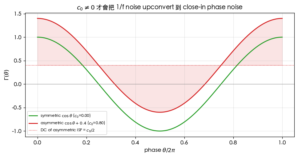
- Asymmetry (e.g. fast rise, slow fall, or even-order harmonics that make the waveform top/bottom asymmetric) shifts the ISF's average away from 0 → .
The figure below overlays a symmetric and an asymmetric ISF: the symmetric one has its DC average pinned at 0, while the asymmetric one is lifted by a "DC offset" of — that offset is the culprit behind flicker upconversion.
Feeding actual device flicker into a simulation makes the close-in difference very clear: the asymmetric waveform shows a steep 1/f³ skirt, while the symmetric waveform shows almost none (only 1/f² and the floor remain).
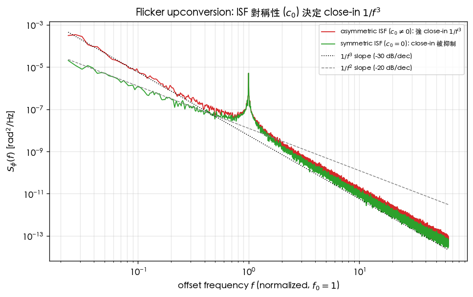
Both figures are pedagogical toy models (not transistor-level): the ISF uses an analytic shape (symmetric , asymmetric , etc.), and flicker is a synthesized 1/f sequence. They faithfully illustrate " determines 1/f³" causally, but are not a measurement of any real transistor. Full scripts:
simulations/lab_05_fourier_isf.py,simulations/lab_07_flicker_noise.py.
Numerical example (building intuition)
The first example uses an assumed (illustrative); the second switches to the closed forms of [P2] Appendix B and computes and the corner directly from the topology parameters — full derivation in asymmetric_isf_closed_form.
Symmetric waveform (): theoretically , and the 1/f³ corner is pushed to extremely low frequency — in practice it is dominated by the small residual set by mismatch (see the knobs table below).
Asymmetric waveform (illustrative, assumed): take , (so ). If the device MHz, then
- Intuition: lowering from 0.4 to 0.04 (10× smaller) drops the corner by 100× () — from 320 kHz down to 3.2 kHz. In other words, each order-of-magnitude improvement in symmetry shrinks the reach of the 1/f³ skirt by two orders of magnitude — an extremely cost-effective design lever.
Asymmetric waveform (computed, directly from ring topology parameters): a ring with , , whose rise is 1.5× steeper than its fall (asymmetry ratio ). The [P2] App. B closed forms (Eq.(55)/(56)/(57), p.803; derivation in asymmetric_isf_closed_form) directly give
- Convention flag: 42.86 kHz is the [P2] Eq.(7)/(57) bookkeeping; substituting
back into [P1] Eq.(24) above yields kHz (a DC-channel weighting convention difference;
see the flag on the new page. Scalings and ratios are unaffected). The numbers are verified by
simulations/lab_33_asymmetry_corner.py(closed forms vs numeric integration, error ). - New design message ([P2]'s own sentence, p.803): at fixed the corner is — rings with fewer stages have a higher flicker corner (at : kHz, kHz). White-region phase noise is approximately N-independent ([P2] Eq.(23)), but the 1/f³ knee is pushed down by the stage count.
- Corresponding experimental evidence: [P2] Fig. 17, p.802 measures ring-oscillator phase noise vs. "symmetry control voltage," which shows a minimum at the symmetry point — direct support for the design rule "symmetric → low 1/f³." (Verified: [P2] Fig. 17, p.802, "Phase noise versus symmetry voltage for oscillator number 7" — the y-axis is the 1/f³ corner frequency, showing a clear dip to a minimum at the symmetry point.)
Design knobs for lowering (checklist)
| Knob | How | Why it lowers | Cost/notes |
|---|---|---|---|
| Symmetric rise/fall | NMOS/PMOS drive-strength or pull-up/pull-down symmetry (ring); differential topology | ISF's upper and lower half-periods cancel → average → 0 | needs sizing/bias tuning; process offset leaves residual |
| Differential / even-harmonic suppression | fully differential, symmetric loads, suppress even harmonics | even harmonics make the waveform top/bottom asymmetric → raise | 2× devices, area, power |
| Symmetric load (ring) | use a symmetric load ([P2]'s approach) instead of a single-ended inverter delay cell | matches rise/fall shape | [P2] Fig. 17's "symmetry voltage" tunes exactly this |
| Reduce DC-bias-point drift | control duty cycle near 50% | duty deviating from 50% means a DC-asymmetric waveform → | needs duty-cycle correction |
| Directly lower device flicker | use large-area, PMOS, buried-channel devices | lowers itself (does not change , but lowers the magnitude of 1/f³) | large area → large parasitic capacitance → lowers |
Note the two categories: the first four knobs change / the corner location; the last one changes the device / the overall height of 1/f³. Both can be used in design, but "making it symmetric" is usually free (no extra power) — take that shot first.
Validity and failure conditions
| Condition | Holds when | Fails when |
|---|---|---|
| Small perturbation, ISF known and fixed | fully determines 1/f³ | under large injection/strong nonlinearity the ISF itself changes |
| Device noise is pure 1/f | the model holds | with RTS/burst noise, a separate calculation is needed |
| Cyclostationarity already folded into the effective ISF | compute using | if is also asymmetric, it can "recreate" a nonzero effective (see device_noise_mapping) |
Important warning: what actually determines the upconversion is the of the effective ISF , not just the of the bare . Even if is symmetric, if the device only "leaks noise" during half the period ( is asymmetric), the effective of can still be nonzero. See device_noise_mapping and effective_isf.
Worked examples
The following two examples demonstrate the most cost-effective design lever — "improving symmetry lowers the 1/f³ corner" — reusing this site's canonical , device MHz. Both use an illustrative assumed (conversion practice); to compute the real from topology parameters , see asymmetric_isf_closed_form.
Example 1 (baseline: compute the 1/f³ corner for an asymmetric waveform; is an illustrative assumed value) Given , , device 1/f corner MHz, find the 1/f³ corner .
Step-by-step substitution (with units), using the just-derived :
- Result: kHz — lower than the device's own 1 MHz corner, because .
- Dimension check: ✓ (a ratio of frequencies works equally in Hz or rad/s, since and the 's cancel).
- One-line Python check (using the canonical conversion;
simulations/common/has no dedicated corner function, so compute it directly):
c0, gamma_rms, f_1f = 0.4, 0.5, 1e6
f_1f3 = f_1f * c0**2 / (2 * gamma_rms**2)
print(f_1f3 / 1e3, "kHz")   # -> 320.0 kHz
Example 2 (improving symmetry by one order of magnitude → corner drops two orders of magnitude) Make the waveform more symmetric so drops from to (10× smaller), with and unchanged. Find the new corner, and express in dB how much the heights of the two 1/f³ asymptotes (extrapolated skirts) differ.
Step-by-step substitution (with units):
The corner drops from kHz → kHz (a 100× reduction the square of the ratio, ). Note that after improvement the corner falls to kHz, so kHz for the improved waveform now lies in the 1/f² region (no longer 1/f³); what follows compares the heights of the two 1/f³ asymptotes (extrapolated skirts). 1/f³ phase noise ([P1] Eq.(23)) , so the change in height is
- Result: lowering by 10× → the 1/f³ skirt overall drops 20 dB, and the corner drops 100× (to 3.2 kHz). "Each order-of-magnitude improvement in symmetry shrinks the reach of 1/f³ by two orders of magnitude" is exactly this law.
- Dimension check: dB is a log of a power ratio (dimensionless) ✓; the corner is still in Hz ✓.
- One-line Python check:
import numpy as np
c0_old, c0_new = 0.4, 0.04
print("corner ratio:", (c0_new/c0_old)**2,            # -> 0.01  (3.2 kHz / 320 kHz)
      "; dL =", 10*np.log10((c0_new/c0_old)**2), "dB") # -> -20.0 dB
Both examples are pedagogical toys (not transistor-level): uses assumed values representing "residual asymmetry." A real circuit's must be extracted from the effective ISF (including cyclostationary ); see device_noise_mapping.
Key takeaways
- Only the ISF's DC coefficient upconverts device 1/f noise into close-in 1/f³ ([P1] Eq.(23)).
- 1/f³ corner , not equal to the device's 1/f corner ([P1] Eq.(24)).
- Symmetric rise/fall → the ISF cancels over one period → → the 1/f³ corner is pushed to very low frequency.
- Lowering by 10× lowers the 1/f³ corner by 100× (): illustrative , MHz → corner 320 kHz.
- A ring's can be computed directly from topology: the [P2] App. B closed forms give and corner (, kHz; [P1] Eq.(24) convention ) — see asymmetric_isf_closed_form.
- Design levers: differential, symmetric loads, 50% duty; must look at the of the effective ISF (including ).
- Experiment: [P2] Fig. 17, phase noise vs. symmetry voltage, shows a minimum.
Further reading
- Full upconversion derivation: flicker_noise_upconversion
- Closed forms for , and the corner of the asymmetric triangular ISF ([P2] App. B): asymmetric_isf_closed_form
- Why 's shape tracks the waveform slope: waveform_slope
- Effective ISF and : device_noise_mapping, effective_isf
- Fourier coefficients and Parseval: fourier_series_of_isf
- Why SerDes cares more about close-in: serdes_clocking_connection