Device noise → ISF harmonics mapping
β: This English translation is in beta — the Traditional-Chinese original is the authoritative version.
Prerequisites: white_noise_to_phase_noise (white → 1/f²), flicker_noise_upconversion (flicker → 1/f³), fourier_series_of_isf (, ) | Next: symmetry, tank_swing, serdes_clocking_connection
This page collects the scattered design intuition from earlier pages into a single map: how does the noise (white and flicker) of one transistor end up as the oscillator's phase noise? The key is two things — which frequency band of device noise is picked up by which ISF harmonic, and the device does not leak noise throughout the entire period (cyclostationary), so what actually matters is the effective ISF .
Physical intuition (conclusion first): think of the ISF as a multi-channel radio. Its Fourier coefficients are the antenna gains of each channel: picks up device flicker "near DC" (upconverted to 1/f³); picks up device white noise "near ", "near ", and so on (downconverted to 1/f²). But the device only actually conducts — only actually leaks noise — during certain phases of the waveform. This "when does it leak" switching function must be multiplied into first, becoming the effective ISF, before it is the radio's true antenna.
Step 1: two "bands" of device noise
The drain current noise of a MOS device (referred to the injection node) splits roughly into two bands ([P1] Eqs.(19),(22), p.185):
- White noise: thermal (-type) + shot, flat with frequency, energy spread over all frequencies, including near .
- Flicker (1/f) noise: slow trap/release processes in the channel, energy concentrated at low frequency (), significant below the device's 1/f corner .
- Units: both bands are A²/Hz.
Step 2: ISF harmonics are "receive channels" — who picks up what
Substitute the ISF Fourier expansion ([P1] Eq.(12)) into the phase response ([P1] Eq.(13)): each term is a mixer that shifts "noise near " down to baseband phase:
| ISF harmonic | Device-noise band received | Shifted to | Resulting phase-noise region |
|---|---|---|---|
| (DC term, value ) | Low-frequency flicker (near DC) | Pure integration, no shift | close-in 1/f³ ([P1] Eq.(23)) |
| White at | Downconverted to | Main 1/f² contribution | |
| White at | Downconverted to | Also feeds 1/f² (via ) |
- White noise → 1/f²: all (the white part, ) contribute together, and via Parseval collapse to ([P1] Eq.(20), p.185), giving ([P1] Eq.(21)). So 1/f² is set by .
- Flicker → 1/f³: only the DC channel receives it, giving ([P1] Eq.(23)). So 1/f³ is set by .
- One-line summary: governs white (1/f²); governs flicker (1/f³). This is the skeleton of the whole map.
The clearest way to see this "multi-channel radio" is a figure: the top half is the device's current-noise PSD (a near-DC flicker bump plus a flat white plateau); three shaded bands mark the frequency ranges the ISF actually "listens to" (DC, , ); the bottom half is the same ISF's Fourier coefficients as a stem plot, aligned under the bands above, with arrows showing each band folding back to the carrier weighted by that harmonic's — upconverts near-DC flicker into close-in 1/f³, while downconvert white noise near into 1/f².
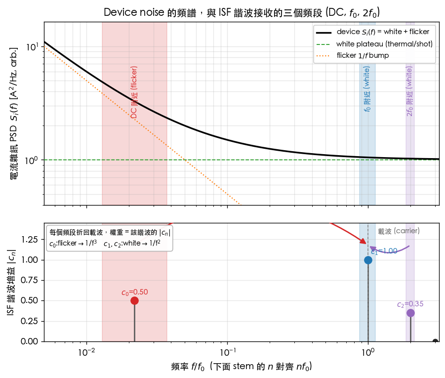
The in the figure are computed by
simulations/fig_device_noise_bands.pyusingcompute_fourier_coefficientson a toy asymmetric ISF (), giving , , . This is a pedagogical toy model (not transistor-level): it only illustrates the "harmonic = channel" mapping structure; the vertical axis is in arb. units. Corresponds to [P1] Eq.(12),(13) (Fourier expansion → per-harmonic phase response) and Eq.(19),(23) (white/flicker summation).
Turning this map's "radio gain" into concrete algebra (this page has had relatively few equations so far; here we fill in the three core relations, all from [P1] and consistent with the site's formula table):
(M1) White → 1/f² phase noise ([P1] Eq.(21), p.185; numerator is ):
(M2) Flicker → 1/f³ phase noise ([P1] Eq.(23), p.185; numerator is ):
(M3) Relative height of the two regions (same offset, divide the linear bracket of (M2) by (M1)):
- Use of (M3): at any given offset, this ratio means flicker (1/f³) dominates, means white (1/f²) dominates; setting it solves for the 1/f³ corner ([P1] Eq.(24), derivation in symmetry).
- Dimension check: the right-hand side of (M3) is = dimensionless ✓ (a pure ratio, correct).
Step 3: cyclostationary — the device does not leak noise all the time
The above is the "bare ISF" — it assumes the noise is equally large at every instant. But a real device's noise strength is periodically varying (cyclostationary): e.g. a tail current source conducts only during part of the cycle, and a switching pair's peaks only during transitions. Hajimiri–Lee describe "when the device is leaking noise" with a noise-modulating function (NMF) (, periodic), folded into the ISF ([P1] Sec. II-D, Eq.(25)–(27), p.186; is Eq.(25), is Eq.(27)):
- Meaning: what actually enters the phase-noise formulas is not but . All of , , must be recomputed using .
- A design-critical consequence: even if waveform symmetry makes the bare 's , if the device leaks noise only during half the cycle ( asymmetric), can regrow a nonzero → flicker gets upconverted again. Conversely, aligning the device's "conduction window " with the low-value phase of the bare can simultaneously lower and .
- A more rigorous mathematical foundation (PPV / adjoint / Floquet) is not in the five downloaded PDFs and is supplemented from standard literature (Demir–Mehrotra–Roychowdhury 2000, etc.); see effective_isf.
A toy calculation using the built-in functions (pedagogical toy model, not transistor-level):
import numpy as np
from simulations.common.isf_utils import (
    gamma_lc_ideal, effective_isf, compute_fourier_coefficients, gamma_rms)

theta = np.linspace(0, 2*np.pi, 2048, endpoint=False)
gamma = gamma_lc_ideal(theta)            # bare ISF = -sin(theta), c0 = 0
# Asymmetric NMF: device conducts only in the first half-cycle (alpha=1 for theta<pi, else 0)
alpha = np.where(theta < np.pi, 1.0, 0.0)
gamma_eff = effective_isf(gamma, alpha)       # multiply by NMF (positional: gamma_values, alpha_values)
a0, a, b, c, ph = compute_fourier_coefficients(theta, gamma_eff, n_harmonics=8)
print("c0 =", a0, " Gamma_rms =", gamma_rms(theta, gamma_eff))
# -> c0 ≈ -0.637 (bare Γ had c0=0; regrown by the asymmetric α), Gamma_rms ≈ 0.500
(Full API in simulations/common/isf_utils.py; effective_isf and gamma_rms are real functions.)
Step 4: two independent levers — which knobs move , which move
The core phase-noise ratios are (white, [P1] Eq.(21)) and (flicker, [P1] Eq.(23)). The numerator (ISF shape) and denominator (charge swing) are two mutually independent knobs. Classifying every design knob by "which quantity it moves":
| Move / (ISF shape) | Move (charge swing) |
|---|---|
| Waveform symmetry (matched rise/fall) → lowers | Increase voltage swing |
| Fast transitions (steep edges) → lowers | Raise tank / (larger swing at the same current) |
| Ring stage count → (below) | Increase node capacitance (ties to ; use with care) |
| Symmetric load, differential → lowers even harmonics, lowers | Differential → 2× effective swing |
| Align device conduction window with low- phase (cyclostationary) → lowers effective , | Push bias to the headroom limit (current/voltage limited) |
| Lower device (larger area, PMOS) → lowers 1/f³ height (does not change ) | — |
The ring's comes from [P2] Eq.(16), p.794 (re-verified in v7: the square root covers only the constant, ; triple-checked against the main text's 4/N^1.5@η=0.75 and Appendix B Eq.(55). v3 had misread this as N^-0.75): ( is the stage-delay proportionality constant), and at fixed and fixed power ring phase noise is roughly independent of (the device count growing with offsets the drop in ) — see lc_vs_ring.
Numerical example (building intuition)
Map a single device's two noise bands onto the two phase-noise regions.
Take canonical values: GHz, pC, , A²/Hz, asymmetric , device MHz.
- White → 1/f² (@ MHz, [P1] Eq.(21)): as in Example B, dBc/Hz.
- Flicker → 1/f³ (@ MHz, [P1] Eq.(23)): relative to 1/f² there is an extra factor . At MHz the two regions cross (); 1/f³ is dB relative to 1/f² — i.e. at this offset the flicker contribution is still slightly below white; the crossover point (1/f³ corner) falls at kHz (see symmetry). Only below 320 kHz does flicker dominate.
- Intuition: at 1 MHz offset flicker is barely visible (masked by white); to see 1/f³ you need to look below 100 kHz. If a SerDes loop bandwidth filters out the close-in region, the 1/f³ impact shrinks (see serdes_clocking_connection).
The full map (mermaid)
Validity and breakdown conditions
| Condition | Holds when | Breaks down when |
|---|---|---|
| Small perturbation, linear LTV | Per-band mapping holds | Strong nonlinearity, large injection — the ISF itself changes |
| Noise separable into white + 1/f | Two regions cleanly separated | RTS/burst/correlated noise needs separate treatment |
| Cyclostationary via | First-order correction is sufficient | When rigorous PPV/adjoint treatment is needed (external literature) |
Worked examples
The following two problems map white and flicker device noise onto phase noise respectively, demonstrating the two independent knobs (governing white) and (governing flicker). Using canonical values: GHz, pC, , A²/Hz, asymmetric , device MHz.
Example 1 (mapping white noise onto → 1/f² height) Use (M1) to compute the 1/f² phase noise at MHz; then ask how much it drops (in dB) if is halved ().
Step-by-step substitution (with units):
Halving → becomes → dB → new value dBc/Hz.
- Result: white noise's 1/f² height dBc/Hz; halving → 6 dB improvement. White depends only on , not on at all.
- Dimension check: same as tank_swing Example 1 — the bracket reduces to a dimensionless per-Hz power ratio → dBc/Hz ✓.
- One-line Python check:
import numpy as np
def L_white(grms, qmax, Si, dw): return 10*np.log10(grms**2/qmax**2 * Si/(4*dw**2))
dw = 2*np.pi*1e6
print(round(L_white(0.5,1e-12,1e-24,dw),1),
      round(L_white(0.25,1e-12,1e-24,dw)-L_white(0.5,1e-12,1e-24,dw),2))  # -> -148.0 -6.02
Example 2 (mapping flicker noise onto → 1/f³ height, using (M3) to determine which region dominates) Use (M2) to compute the 1/f³ phase noise at kHz, and use (M3) to determine whether that offset is dominated by flicker or white.
Step-by-step substitution (with units), first computing the (M3) ratio to determine which dominates ( kHz ):
Ratio → at 100 kHz flicker already dominates (consistent with the corner kHz kHz). The flicker height itself:
- Result: at 100 kHz, 1/f³ (flicker) is about dBc/Hz and dominant (ratio 3.2). Flicker depends only on : if symmetrizing the waveform brings (10× smaller), this 1/f³ curve drops by dB overall.
- Dimension check: the (M3) ratio is dimensionless ✓; (M2)'s bracket has an extra dimensionless factor , changing the slope to (1/f³) ✓.
- One-line Python check:
import numpy as np
c0, grms, qmax, Si, f1f = 0.4, 0.5, 1e-12, 1e-24, 1e6
df = 1e5; dw = 2*np.pi*df
ratio = c0**2/(2*grms**2) * (f1f/df)
L_1f3 = 10*np.log10(c0**2/qmax**2 * Si/(8*dw**2) * (f1f/df))
print(round(ratio,2), round(L_1f3,1))   # -> 3.2  -123.0  (ratio>1 => flicker dominates)
Both problems are pedagogical toys (not transistor-level): and use assumed values. A real circuit must recompute , using the effective ISF (see Step 3 and effective_isf).
Key takeaways
- Device noise has two bands: white (spread over all frequencies), flicker (concentrated at low frequency).
- ISF harmonics are receive channels: receives flicker → 1/f³; receive white → 1/f² (collapsed to via Parseval).
- What actually matters is the effective ISF (cyclostationary); a symmetric bare can regrow because of an asymmetric .
- Two independent levers: move / (waveform symmetry, fast edges, differential, alignment) vs. move (swing, , differential).
- Ring ([P2] Eq.(16), p.794, re-verified in v7: the square root covers only the constant); at fixed /power, phase noise is roughly independent of .
Further reading
- Effective ISF and PPV/adjoint: effective_isf
- White → 1/f²: white_noise_to_phase_noise
- Flicker → 1/f³: flicker_noise_upconversion
- and Parseval: rms_isf
- lever: tank_swing; symmetry: symmetry
- Correlated supply/substrate noise shuts down channels of this map at once, leaving only DC and ([P2] Eqs.(37)–(38) selection rule): lab_34_correlated_supply