β: This English translation is in beta — the Traditional-Chinese original is the authoritative version.
From ISF to SerDes Clocking
Prerequisites: psd_phase_noise_jitter (, , the four jitter "dialects," and phase↔time conversion), tank_swing ( sets the VCO's own noise), lc_vs_ring (accumulated jitter and the LC/ring trade-off) | Next: pll_noise_budget, exercises
This is the capstone page of Chapter 06: it connects everything said so far about ISF / phase noise to what a SerDes (serializer/deserializer, high-speed serial transceiver) designer looks at every day — clock jitter, eye opening, BER (bit error rate). We derive, step by step, the two phase→time conversions, clarify how to choose the integration bandwidth, the difference between RJ and DJ, and why a CDR/PLL behaves like a high-pass filter that removes the VCO's close-in noise — which is why "the same VCO behaves completely differently under different loops."
Physical intuition (conclusion first): an oscillator's phase noise is "the phase jittering." What a SerDes designer cares about is "how much the edge jitters on the time axis" and "the probability that the sampling instant lands near the center of the eye." Phase jitter → time jitter () → the sampling point drifts off the eye center → the eye narrows → BER worsens. But not all phase noise, regardless of frequency, is harmful: the CDR/PLL tracks slow phase drift (low-frequency noise is absorbed by the loop), leaving only the fast noise the loop cannot follow to become jitter. So "integration bandwidth" and "loop bandwidth" are the two central knobs of SerDes clocking.
Step 1: phase → time (a single phase error)
How does an oscillator's excess phase turn into an edge timing error? One period corresponds to rad of phase, so phase and time are proportional (notation, Eq. 17):
Step-by-step derivation: the signal is . Treat a perturbation of as a time shift : requiring and solving gives , i.e.
- Dimension check: ✓ ( has units of rad/s, not Hz).
- Intuition (5 GHz): 1 mrad → 31.8 fs; 1 rad → 31.8 ps (≈ , sensible).
Step 2: phase PSD → rms jitter (needs an integral)
A single is not useful — jitter is the sum of phase noise across all frequencies. First integrate the phase PSD to get phase variance (Eq. 18):
Then use Step 1 to convert rms phase to rms time (Eq. 19):
Step-by-step explanation:
- Why integrate: is "phase power per Hz" (rad²/Hz). Phase jitter at different offset frequencies is independent, so the powers add — integrating over gives the total phase variance (rad²).
- Dimension check: ✓ → take the square root to get rad.
- Convert to time: divide by (rad/s) → s.
- Connecting to measurement: a phase-noise analyzer reports (dBc/Hz); use the small-angle approximation (the factor-of-2 for single-sided → double-sided, Eq. 16) to convert to before integrating.
The figure below shows rms jitter obtained by integrating (5 GHz, dBc/Hz @ 1 MHz, 1/f², integrated 1→100 MHz):
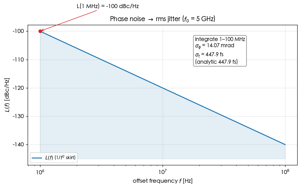
This figure is not a toy model (it is the standard SerDes jitter-integration procedure). Full script:
simulations/lab_08_jitter_integration.py. Numerical integration matches the closed-form result exactly.
Step 3: numerical example (canonical example C)
GHz, dBc/Hz, 1/f² slope, integrated 1→100 MHz.
- dBc/Hz→: dBc/Hz ; rad²/Hz.
- 1/f² shape: .
- Integral: rad² → mrad.
- Convert to jitter: fs.
Key intuition: the 1/f² integral is dominated by the lower limit (the term is largest) — so "where you start integrating from" is critical. This is exactly the meaning of "integration bandwidth" and "CDR high-pass" discussed below. See numerical_feeling Example 3 for the full mental-math walkthrough.
Step 4: how jitter eats into eye opening and BER
The SerDes receiver samples at the center of each bit. Let the bit period (UI, unit interval) be . Timing jitter at the sampling instant directly "eats into" the eye's horizontal opening from both sides. For the case of RJ (Gaussian) only, the BER at an offset from the eye center is a bathtub curve (standard SerDes model, §10.2 of the spec):
-
How to read it: the two terms are, respectively, the probability that "the left edge (at ) jitters past the sample point on the right" and that "the right edge (at ) jitters past the sample point on the left." At the exact eye center the two terms are equal and BER is lowest (the bottom of the bathtub).
-
Solving for eye opening from BER: to meet a target BER (e.g. ), the one-sided margin at the bottom () must satisfy . With :
-
Eye horizontal opening (one-sided) , where is the inverse Gaussian Q-function value for the target BER (e.g. BER → , total RJ ≈ peak-to-peak).
-
Intuition: RJ is Gaussian and unbounded, so the stricter the BER target (the smaller the probability), the more margin must be reserved (larger ). Each increment of eats off each side of the eye.
-
Order of magnitude: in the example above, fs; at GHz, if the data rate is 10 Gb/s ( ps), the RJ overhead for BER is ps UI — clock RJ alone eats 6.3% of the eye. This is why high-speed links are so sensitive to VCO phase noise.
⚠️ The -value and -UI-opening eye/BER model is standard SerDes/communications knowledge (not in the five downloaded PDFs; supplemented from standard literature, e.g. the dual-Dirac jitter model, OIF-CEI, Razavi). [P1]/[P2] provide phase noise/jitter itself; they do not cover link budget.
Step 5: the difference between RJ / DJ / accumulated jitter
What a SerDes measures as "jitter" is actually several components stacked together, and they are treated completely differently (see the "four dialects" in notation):
| Type | Source | Statistics | How it enters BER |
|---|---|---|---|
| RJ (random jitter) | oscillator phase noise, thermal | Gaussian, unbounded, characterized by | peak-to-peak ; margin grows with stricter BER |
| DJ (deterministic jitter) | ISI, duty-cycle distortion, crosstalk, PSIJ | bounded, characterized by peak-to-peak | added directly (bounded), does not scale with BER |
| period jitter | single-period length deviation | — | clock internal spec |
| cycle-to-cycle | adjacent-period difference | — | sensitive to PLL stability |
| accumulated / long-term | free-running drift, | random walk | open-loop only; suppressed once CDR/PLL is locked |
- total jitter (TJ) @ BER: (dual-Dirac approximation; for the rigorous version and the gap between , see dj_dual_dirac).
- ISF directly governs RJ and accumulated jitter (they originate from phase noise); DJ is mostly a link/pattern issue that ISF cannot see.
Step 6: CDR/PLL high-pass filtering of VCO phase noise (the key point)
This is the single most important idea on this page, and the answer to "why the free-running does not grow without bound in practice."
- Put the VCO inside a PLL (locked to a clean reference) or a CDR (locked to data edges), and the loop tracks the VCO's slow phase drift: as long as the drift is slow enough (offset frequency below the loop bandwidth ), the loop corrects it.
- The result is that the VCO's own phase noise experiences a high-pass transfer function:
- Conversely, the reference clock (or the CDR's input data-edge) noise experiences a low-pass: low frequencies pass unchanged, high frequencies are filtered out.
- Design consequences:
- The integration lower limit should be taken near the loop bandwidth (not DC) — because VCO noise below has already been absorbed by the loop. This directly answers "how to choose the integration bandwidth": closed-loop jitter is integrated from to (Nyquist or half the data rate).
- Accumulated jitter is truncated: the free-running random walk (, energy concentrated at very low frequency) falls exactly in the high-pass stopband → it is suppressed into a bounded tracking error. So once locked, it no longer drifts without bound.
- Loop bandwidth is a trade-off: raising → filters out more VCO close-in noise (good), but lets more reference/input noise and the loop's own noise through (bad). The optimal sits near the crossover point of the VCO-noise and reference-noise curves.
⚠️ The PLL/CDR high-pass/low-pass transfer function is standard PLL theory (not in the five downloaded PDFs; supplemented from standard literature, e.g. Gardner, Razavi, Best). [P1]/[P2] cover open-loop oscillator phase noise theory; this section is the bridge to closed-loop clocking. TODO: manual verification needed — for an exact loop transfer function (including charge-pump and loop-filter order), consult standard PLL literature.
Step 7: practical intuition for TX PLL / RX PLL / LC-VCO / ring-VCO
| Scenario | Intuition | LC or ring? |
|---|---|---|
| TX PLL (generates the transmit clock) | Directly sets transmit jitter; usually narrow loop BW (absorbs ref noise), so VCO close-in noise matters | High-speed lanes use LC-VCO (low phase noise); jitter requirements are strict |
| RX CDR (recovers clock from data) | Loop BW is set by data/jitter tolerance; high-passes away VCO close-in | Commonly uses ring-VCO (wide tuning, multi-phase, small area — and close-in is filtered by the CDR, so it is less fatal) |
| LC-VCO | Low , low phase noise, slow drift; large area, narrow tuning | TX, reference, high performance |
| ring-VCO | Worse phase noise, faster jitter accumulation; but wide tuning, naturally multi-phase, small area; close-in is suppressed once inside a fast loop | RX CDR, low-power/area-sensitive, multi-phase needs |
- Core trade-off: the ring's weakness (close-in 1/f³, fast random walk) falls exactly in the loop's high-pass stopband — if the loop bandwidth is wide enough, the ring-VCO's close-in weakness is largely compensated. This is why many RX CDRs use ring instead of LC.
- Conversely, a TX PLL often uses a narrow loop to filter out reference spurs, so VCO close-in noise appears directly at the output → LC is preferred.
The spec's 10 required design questions — summary table (with cross-page links)
| # | Question | One-line answer | Details |
|---|---|---|---|
| 1 | Why does symmetry affect flicker upconversion? | Only the ISF's upconverts flicker; a symmetric waveform has | symmetry |
| 2 | Why does swing lower phase sensitivity? | , ; doubling swing → −6 dB | tank_swing |
| 3 | Why is injection dangerous where the slope is small? | ; small slope → large → high phase sensitivity | waveform_slope |
| 4 | How do LC and ring compare? | LC: high /large /low noise; ring: more devices/ISF concentrated at transitions; at fixed /P, ring is ~independent of | lc_vs_ring |
| 5 | How is ISF related to jitter? | sets both phase noise and () | lc_vs_ring, this page §2 |
| 6 | How is phase noise integrated into jitter? | ; 1/f² dominated by the lower limit | this page §2–3, numerical_feeling |
| 7 | Knobs to change ? | Waveform symmetry, fast edges, differential, aligning cyclostationary , increasing ring | device_noise_mapping |
| 8 | Knobs to change ? | Increase swing , raise tank /, differential, push toward headroom | tank_swing |
| 9 | How to lower white-noise (1/f²) phase noise? | Lower , raise , lower ([P1] Eq.21) | tank_swing, device_noise_mapping |
| 10 | How to lower flicker close-in (1/f³)? | Lower (symmetric/differential/50% duty/ alignment), lower device , rely on loop high-pass | symmetry, this page §6 |
Validity and failure conditions
| Condition | Holds when | Fails when |
|---|---|---|
| Small-angle approximation | rad | large phase jitter (near 1 rad): SSB↔PSD diverges |
| RJ Gaussian and independent of DJ | dual-Dirac TJ model valid | non-Gaussian RJ or correlated jitter: needs jitter decomposition |
| loop transfer is first-order high-pass | intuitive estimate of the integration lower limit | higher-order loop or peaking: need the full transfer function |
| open-loop ISF theory | computing the VCO's own phase noise | closed-loop: must stack loop filtering on top |
Worked examples
The following two examples work through this page's two core operations in detail: (1) using and the Q-function to compute the BER bathtub opening (UI=100 ps); (2) integration-bandwidth choice — how much jitter differs when the lower limit is taken at DC vs. the loop bandwidth. We reuse the canonical case: GHz, dBc/Hz, 1/f² slope, example C gives fs.
Example 1 (compute the BER bathtub opening from , UI=100 ps) Data rate 10 Gb/s → UI ps. Clock RJ fs (example C, assuming no ISI/DJ). Find: (a) the BER at the exact eye center ; (b) the bathtub's horizontal opening (eye opening) needed to guarantee BER .
Step-by-step substitution (with units). First compute how many 's the center-to-edge distance is relative to :
(b) The opening is set by "how far from center BER rises to ." , so the tolerable one-sided offset satisfies :
- Result: (a) center BER is astronomically small ( is only of half a UI); (b) the BER bathtub opening ps UI — i.e., clock RJ eats ps from each side, ps UI total. Consistent with Step 4's "448 fs RJ ≈ 0.063 UI."
- Dimension check: 's argument is dimensionless ✓; opening divided by UI gives a UI count (dimensionless) ✓.
- One-line Python check (using the real
Qandber_bathtubfromsimulations/common/serdes_utils.py):
import numpy as np
from simulations.common.serdes_utils import Q, ber_bathtub
ui, sigma_t = 100e-12, 447.9e-15
print("BER(0) =", ber_bathtub(0.0, sigma_t, ui))          # -> ~0 (1e-300 floor)
t_edge = ui/2 - 7.03*sigma_t
print("opening =", 2*t_edge*1e12, "ps =", 2*t_edge/ui, "UI")  # -> 93.7 ps = 0.937 UI
Example 2 (integration-bandwidth choice: lower limit at DC vs. loop bandwidth) Same VCO (example C's 1/f² skirt, rad²/Hz), upper limit MHz. Compare rms jitter from "open-loop, integrated from kHz" vs. "closed-loop, integrated from loop bandwidth MHz." This is the numerical version of "why CDR/PLL high-pass reduces jitter."
Step-by-step substitution (with units). The 1/f² phase-variance integral has closed form ; here :
- Result: raising the integration lower limit from 10 kHz (open-loop) to 1 MHz (loop BW) → rms jitter drops from 4.50 ps to 448 fs (roughly a reduction). Because the 1/f² jitter is dominated by the lower limit , the loop's high-pass removes VCO close-in noise below , equivalent to raising the integration lower limit to — this is the quantitative answer to "how to choose the integration bandwidth": closed-loop jitter is integrated from to .
- Dimension check: ✓; ✓.
- One-line Python check (using
simulations/common/noise_utils.py):
import numpy as np
from simulations.common.noise_utils import leeson_one_over_f2, integrate_rms_jitter
for f1 in (1e4, 1e6):
    f = np.logspace(np.log10(f1), 8, 6000)
    L = leeson_one_over_f2(f, L_ref_dbc=-100, f_ref=1e6)
    st, sp = integrate_rms_jitter(f, L, f0=5e9, fmin=f1, fmax=100e6)
    print(f"f1={f1:.0e}: sigma_t = {st*1e15:.1f} fs")
# f1=1e+04: sigma_t = ~4500 fs ; f1=1e+06: sigma_t = 447.9 fs
Example 1's BER/Q model is standard SerDes knowledge (not in the five PDFs; supplemented from standard literature, e.g. dual-Dirac, OIF-CEI); Example 2's loop high-pass truncation is standard PLL theory (not in the five PDFs). The phase noise/jitter itself comes from [P1]/[P2].
Key takeaways
- ; (1/f² is dominated by the lower integration limit).
- Example C: dBc/Hz @ 1 MHz, 5 GHz, 1/f², 1→100 MHz → mrad, fs.
- Jitter eats the eye from both sides: /side; at 10 Gb/s, BER : 448 fs RJ ≈ 0.063 UI.
- RJ (Gaussian, from phase noise, governed by ISF) vs. DJ (bounded, ISI/crosstalk, invisible to ISF); TJ DJRJ.
- CDR/PLL is high-pass to VCO noise: close-in/accumulated jitter is suppressed → integration lower limit ≈ .
- Practice: TX PLL favors LC-VCO (close-in matters); RX CDR often uses ring-VCO (close-in filtered by the loop).
Further reading
- Jitter types and PSD: psd_phase_noise_jitter
- Mental-math exercises: numerical_feeling
- LC vs. ring and accumulated jitter: lc_vs_ring
- Design knobs: symmetry, waveform_slope, tank_swing, device_noise_mapping
- Notation and units: notation