ADC aperture jitter: how clock jitter eats SNR and ENOB
β: This English translation is in beta — the Traditional-Chinese original is the authoritative version.
Prerequisites: psd_phase_noise_jitter (the four-step chain), lab_08_jitter_integration (how the 447.9 fs is integrated) | Next: serdes_clocking_connection, exercises
The problem: you swapped in a 12-bit ADC — why didn't the high-frequency SNR improve at all?
A high-speed ADC (analog-to-digital converter) "freezes" the input voltage at the sampling instant. But the sampling instant itself is not ideal: the sampling clock has jitter, and the trigger instant of the sampling switch carries its own random uncertainty — the two combined are called aperture jitter (the rms random error of the sampling instant, , in s). As the input frequency rises, the waveform slope steepens, and the same timing error is amplified by that slope into an ever larger voltage error — beyond some input frequency the SNR is completely pinned by clock quality, regardless of how many bits of ADC you bought.
This page does four things:
- Derive the signature formula step by step from first principles;
- Derive the ENOB (effective number of bits) conversion ;
- Use this site's canonical Example C value fs to compute an honest design table (1 / 2.5 / 5 / 10 GHz), and back-solve "how clean a clock does 10 ENOB @ 5 GHz require";
- Connect it back to this site's main thread: integrate SNR — the oscillator's phase noise plot directly sets the data converter's effective number of bits.
External-literature note: the aperture-jitter SNR formula is a standard data-converter textbook result (external literature, not among the five source PDFs); e.g. W. Kester, "MT-007: Aperture Time, Aperture Jitter, Aperture Delay Time—Removing the Confusion," Analog Devices Tutorial MT-007, 2008; R. H. Walden, "Analog-to-digital converter survey and analysis," IEEE J. Sel. Areas Commun., vol. 17, no. 4, pp. 539–550, Apr. 1999. The input number fs on this page, however, is this site's own verified canonical Example C (lab_08).
Physical intuition (conclusion first): sampling error = slope × timing error. The steepest slope of a sine is (V/s), so the same clock (the same ) hitting an input at twice the frequency gives twice the voltage error and 4× the noise power — SNR drops 6 dB per octave, i.e. 1 bit per octave. This is why in direct RF-sampling systems the most expensive part is often not the ADC itself, but the low-noise clock that feeds it.
Step 1: the voltage error of jittered sampling (error = slope × timing error)
Write down the signal and the sampling instants. Let the ADC sample a full-scale sine:
where is the amplitude (V) and the input frequency (Hz). The ideal sampling instants are (, s); the actual sampling instants carry an additional random error (s):
Extract the error with a first-order Taylor expansion. Because is tiny (fs scale), expand around , keeping only the first order:
- Math used: .
- Unit check (term by term): (V) (rad/s) (s) V·rad; rad is dimensionless, so is in V ✓. The slope has units of V/s — "how many volts of change per second"; multiplied by "how many seconds off", you naturally get volts.
- Validity condition of the first-order approximation: the second-order Taylor term relative to the first is , so we need rad. The worst case on this page (10 GHz, 447.9 fs) is rad ✓, far below 1.
- Physical meaning: this step is the core of the whole page — a timing error is amplified by the waveform slope into a voltage error. The slope is proportional to , so the damage is proportional to . This is the same physical quantity, seen from the other side, as waveform_slope's point that inside an oscillator "the steeper the slope, the less sensitive to noise": inside the oscillator, a steep slope is good (voltage noise converted to phase noise gets divided by the slope); at the sampling interface, a steep slope is bad (the timing error gets multiplied by it).
Step 2: mean-square over jitter and sampling phase → noise power
Now turn the single-sample error into a statistical noise power. Assume (Section 5 below audits each item):
- is zero-mean Gaussian, independent between samples (white RJ), with variance (s²);
- is independent of the signal phase (the jitter does not know where the waveform currently is).
Take the expectation of ; because and are independent, the expectation factorizes:
Where that comes from: the sampling phase sweeps uniformly over a full period (coherent sampling over an integer number of periods, or treating the phase as uniformly distributed), and the average of is — the same fact as "the power of a sine is half the amplitude squared". So the noise power (V²) is:
- Dimension check: (rad dimensionless) ✓.
- Physical meaning: the error is largest at the zero crossings (steepest slope, ), and at the peaks (zero slope, ) jitter is completely harmless — this is exactly the LTV sensitivity idea of [P1] replayed at the sampling interface: "when you get hit" determines how much it hurts (compare lab_02's LC ISF: an oscillator is most sensitive to charge perturbations at the zero crossings — the same / geometry). The is just the average of "sometimes hit on the steep part, sometimes on the flat part".
Step 3: SNR — the signature formula
The power of the sine signal itself is
SNR (signal-to-noise ratio) is the ratio of the two. Note that and the two 's all cancel:
In dB (a power ratio; the square comes out as 20):
- Dimension check: (rad/s) × (s) rad, dimensionless ✓ — the argument of a log must be dimensionless, automatically satisfied here. SNR itself is a power ratio, dimensionless ✓.
- Physical reading (the single most important sentence): is the "timing jitter converted to an equivalent rms phase error on the input sine", (rad). So this formula is really saying: — when sampling a sine, the SNR is the inverse square of the equivalent phase jitter.
- The elegant connection to this site's main thread: the clock's own rms phase at is ; applied to an input at frequency , the equivalent phase scales as . When GHz, the SNR is directly dB — Example C's 14.07 mrad becomes the ADC's SNR unchanged.
- Validity/failure: holds only when rad (the first-order Taylor of Step 1) and jitter is the only noise term; full conditions in Section 5.
Step 4: ENOB — converting to an "effective number of bits"
To phrase SNR in the language of ADC designers, first derive the SNR of an ideal N-bit quantizer (an external standard result: W. R. Bennett, "Spectra of quantized signals," Bell Syst. Tech. J., vol. 27, pp. 446–472, Jul. 1948 (external literature, not among the five source PDFs); derived self-contained here).
(a) Quantization noise power . Let the LSB (least significant bit, the smallest quantization step) be (V). The quantization error is approximately uniformly distributed over , with power (variance):
(b) Full-scale sine power. The full-scale range of N bits is (V), so the sine amplitude is , with power:
(c) Divide and take dB.
- Dimension check: cancels top and bottom, SNR dimensionless ✓; is a bit count (dimensionless).
(d) Invert to define ENOB. Plug any SNR (here the jitter-limited one) back into this formula and solve for : that is "how many bits of ideal quantizer this ADC is equivalent to":
- Validity/failure: assumes the quantization error is uniform and signal-independent (true only for a busy signal; for very small or DC inputs it becomes a deterministic error and requires dither); ENOB is defined against a full-scale sine — back off the input by some dB and the SNR drops by the same dB.
- Composition rule: in a real ADC, jitter, quantization, and thermal noise add in power: . At low frequency quantization/thermal noise dominates and SNR is flat versus ; at high frequency the jitter term comes down at dB/dec and takes over — the crossover is the boundary of "how many ADC bits this clock deserves".
Step 5: factor-of-2 bookkeeping check (against this site's conventions)
This site asks of every 2: "where does it come from, and which convention is it?" This formula has three places to check:
- The formula itself hides no 2. The in the numerator (sine power) and the in the denominator (sampling-phase average) cancel each other; the is a genuine angular-frequency conversion (Hz→rad/s), not a bookkeeping convention. So does not depend on SSB/DSB or any convention of .
- The convention hides upstream of . This site's fs is integrated from the measured dBc/Hz using (the small-angle SSB convention ) (psd_phase_noise_jitter, Step 2). As long as is a measured quantity, this conversion is site-wide consistent and unambiguous.
- If is "predicted" from circuit noise, /2-vs-/4 enters. This site's Example B ( GHz, , pC, A²/Hz) with [P1] Eq. (21), p.185 (SSB, convention) gives dBc/Hz; with the time-domain bookkeeping it is dBc/Hz (see white_noise_to_phase_noise). Numerical cross-check: a 3 dB difference in → differs by → differs by dB. However many dB the convention shifts, that shift propagates unchanged into the SNR — pick a convention and stay consistent along the whole chain, or the numbers are meaningless.
Assumptions and failure conditions (an honest list)
| Assumption | Why it is needed | What happens when it fails |
|---|---|---|
| White RJ ( i.i.d. Gaussian) | Noise power spreads uniformly across the Nyquist band (a flat floor in the FFT) | A free-running clock's jitter is colored ( skirt, accumulation, [P2] Eq. (8), p.792): the total-SNR formula still holds (as long as is the total rms over the same integration bandwidth), but the noise concentrates into a skirt beside the signal instead of a flat floor; which close-in components "count" depends on whether the system tracks them out (see design knobs) |
| First-order Taylor ( rad) | Error linear in | Higher-order terms appear; carrier power leaks away as ; at 447.9 fs, GHz is needed to reach rad |
| Jitter independent of the signal | Expectation factorizes | If the clock and the signal share a source (signal derived from the clock), part of the jitter is common-mode and cancels — measured SNR is actually better |
| Full-scale sine, coherent sampling | The standard reference for SNR/ENOB definitions | Back off the input by x dB → SNR drops x dB; a non-coherent FFT needs windowing, with leakage accounted separately |
| No quantization/thermal noise (jitter only) | Isolates a single mechanism | Real ADCs combine powers per Step 4 (d) |
| = RSS of clock RJ + the ADC's internal aperture jitter | Variances of two independent Gaussian sources add | Counting only the clock and forgetting the ADC's internal contribution (the aperture-jitter line item in the datasheet) overestimates SNR |
Design table: a 447.9 fs clock hitting different
Use this site's canonical Example C value fs (5 GHz, dBc/Hz @ 1 MHz, ,
integrated 1→100 MHz; lab_08). The table below is printed by
simulations/lab_30_aperture_jitter.py (simulation verification in the next section):
| [rad] | [dB] | ENOB [bit] | |
|---|---|---|---|
| 1 GHz | 51.01 | 8.18 | |
| 2.5 GHz | 43.05 | 6.86 | |
| 5 GHz | 37.03 | 5.86 | |
| 10 GHz | 31.01 | 4.86 |
One row worked by hand (5 GHz) as a worked example:
- Dimension check: Hz×s = dimensionless (rad once the is attached) ✓; dB and bit are both dimensionless ✓.
- One-line Python verification:
import numpy as np
print(-20*np.log10(2*np.pi*5e9*447.9e-15))            # -> 37.03
print((-20*np.log10(2*np.pi*5e9*447.9e-15)-1.76)/6.02) # -> 5.86
Scaling intuition (reading the table as one straight line):
- Each octave of : SNR dB, ENOB bit — in the table, 5→10 GHz is exactly (6.02 dB apart) and (1.00 bit apart) ✓.
- 1→10 GHz is octaves: bit ✓, fully self-consistent.
- Every 10× improvement in : SNR dB, ENOB bit. The clock and the input frequency are perfectly dual knobs (both enter through ).
- Intuition cross-check (Example B's ideal limit): if the clock were Example B's "single-white-noise-source ideal LC" ( dBc/Hz, [P1] Eq. (21) SSB /4 convention), over the same integration bandwidth shrinks by × → about 1.8 fs → 5 GHz input SNR dB, ENOB bit (with the /2 convention, dBc/Hz gives 82.0 dB, 13.3 bit — Section 5's 3 dB again). A real oscillator has multiple noise sources, flicker, and a buffer chain, and never reaches this ideal.
Inverse design: for 10 ENOB @ 5 GHz, how clean must the clock be?
Problem: the system must retain 10 effective bits on an GHz input (jitter as the only contributor); find the aperture-jitter ceiling .
Step 1 (ENOB→SNR):
Step 2 (invert the formula): from ,
Step 3 (evaluate):
- Dimension check: numerator dimensionless (rad), denominator rad/s → quotient is s ✓.
- One-line Python verification:
import numpy as np
print(10**(-(6.02*10+1.76)/20)/(2*np.pi*5e9)*1e15)   # -> 25.40
Translating the requirement back into phase-noise language (which is how you talk to the oscillator designer): must be squeezed from 447.9 fs to 25.4 fs, a factor of , i.e. the entire skirt shifted down by dB — over the same integration bandwidth (1→100 MHz) this requires
Read through the scaling of [P1] Eq. (21), p.185, : 24.9 dB × in power ratio, to be pieced together from all three knobs — (swing × capacitance, see tank_swing), (waveform symmetry/topology, see lc_vs_ring), and the noise source — or by using a PLL to filter out the close-in part (see design knobs). Honesty note: 25.4 fs is already an "excellent" clock — in order of magnitude, the best commercial RF-sampling clock chains land at integrated jitter of a few tens of fs (an order-of-magnitude statement, not a precise citation), so "10 ENOB @ 5 GHz" is a spec that hugs the practical limit.
The full chain: from the phase-noise plot to ENOB
The first four boxes are exactly the four-step chain of psd_phase_noise_jitter (Example C); this page merely appends the last two. The whole chain in a few lines of Python (reusing lab_08's library):
import numpy as np
from simulations.common.noise_utils import leeson_one_over_f2, integrate_rms_jitter

f = np.logspace(6, 8, 4000)                             # 1 MHz -> 100 MHz
L = leeson_one_over_f2(f, L_ref_dbc=-100, f_ref=1e6)    # 1/f^2 skirt (Example C)
sigma_t, _ = integrate_rms_jitter(f, L, f0=5e9, fmin=1e6, fmax=100e6)
print(sigma_t*1e15)                                     # -> 447.9
print(-20*np.log10(2*np.pi*5e9*sigma_t))                # -> 37.03
An honest warning about integration bandwidth (continuing the psd page's "the lower limit dominates"): Example C's 447.9 fs is the "integrated 1→100 MHz" number. For an ADC, "which offset frequencies count as jitter" depends on observation length and system architecture: an FFT record lasts , and phase drift slower than looks like a frequency offset rather than a noise floor; if the clock is cleaned by a PLL, the close-in part is taken over by the reference. Change the integration bandwidth and changes, and the SNR with it — when reporting a jitter-limited SNR, the integration bandwidth of must be reported with it.
Simulation verification: lab_30 (Monte-Carlo sampling + FFT)
Theory only counts once it has sparred with a "method that does not know the answer". simulations/lab_30_aperture_jitter.py
runs exactly this experiment: sample a unit sine at ( white Gaussian,
fs), rectangular-window coherent FFT (signal placed on an odd bin,
coprime with the -point record, so every sample hits a distinct phase), measure
then overlay it with .
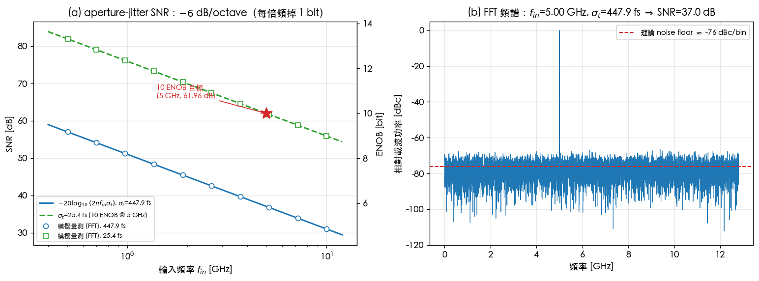
How to read this figure:
- (a): the solid blue line is the formula ( fs), blue circles the FFT measurement — all 10 sweep points fall on the line; the green dashed line/green squares are the same experiment at fs, and the red star is the "10 ENOB @ 5 GHz (61.96 dB)" spec point, which lands exactly on the green line — the inverse design verified closed-loop. The right axis is graduated directly in ENOB: dB/octave reads as "1 bit lost per octave".
- (b): a single spectrum at GHz. The jitter noise is a flat floor (visual evidence of the white-RJ assumption), at about dBc/bin — i.e. the total noise dBc spread over bins () ✓. If the jitter were colored (a real free-running clock), this floor would become a skirt beside the signal, with the total power unchanged.
Actual output (run PYTHONPATH=. python3 simulations/lab_30_aperture_jitter.py):
Monte-Carlo vs formula (same actual coherent f_in):
  f_in =  1.0016 GHz : measured  51.00 dB, formula  51.00 dB, diff -0.00 dB
  f_in =  5.0016 GHz : measured  37.03 dB, formula  37.03 dB, diff +0.00 dB
Core code (full script in simulations/lab_30_aperture_jitter.py):
m = int(round(f_in_target * n / fs))
if m % 2 == 0:
    m += 1                                      # odd bin -> coherent and coprime with 2^14
f_in = m * fs / n
dt = rng.standard_normal(n) * sigma_t           # white Gaussian RJ [s]
x = np.sin(2*np.pi*f_in*(np.arange(n)/fs + dt)) # jittered sampling
p = np.abs(np.fft.rfft(x)/n)**2
snr_db = 10*np.log10(p[m] / (p[1:].sum() - p[m]))
| Parameter | Value | Unit | Notes |
|---|---|---|---|
| 447.9 (second set: 25.4) | fs | canonical Example C; inverse-design spec point | |
| 25.6 | GS/s | Nyquist 12.8 GHz covers GHz | |
| samples | coherent record length | ||
| 0.5–10 (10 sweep points) | GHz | placed on odd bins | |
| Averages | 10–20 | runs | pushes the statistical error of the noise-power estimate down to ~0.02 dB |
| 1 | V (normalized) | full-scale sine; SNR independent of |
Limitations of the simulation (honesty note): this is a pedagogical model — no quantizer (infinite bits), no thermal noise, jitter is white i.i.d. (real clocks are colored; total SNR unchanged, spectral shape changes), and sampling is ideal and instantaneous (no track-and-hold bandwidth roll-off). It verifies the formula itself, not any specific real ADC. Also, the simulation samples the exact value of (not the first-order Taylor), so "measurement = formula to 0.01 dB" simultaneously validates the first-order approximation for rad.
Design knobs: what you can turn in a jitter-limited system
- The clock source itself: ([P1] Eq. (21), p.185) — raise (swing, tank capacitance), pick symmetric waveforms to suppress , replace the ring with an LC (representative value ; true LC ; rings worse, see lc_vs_ring).
- PLL loop bandwidth: inside the loop, close-in noise is taken over by the reference; outside the loop it belongs to the VCO — the optimum bandwidth minimizes the integrated jitter (pll_noise_budget).
- Every stage of the clock chain: buffers, dividers, distribution all add jitter into the RSS; the ADC datasheet's internal aperture jitter is one more term. The budget must be apportioned from .
- Lower the seen at the sampling interface: mixing down before sampling (IF sampling) trades mixer complexity for clock spec — every octave down buys 1 bit.
- Oversampling + digital filtering: white jitter noise spreads flat across the Nyquist band; filtering out the out-of-band part buys of processing gain. But colored (close-in skirt) jitter hugs the signal and cannot be filtered — one more example of "the white/colored assumption decides the answer".
- Waveform slope: sharpening the clock edges (limiting, buffering) suppresses the clock chain's own additive-noise-to-jitter conversion (waveform_slope), but is powerless against phase noise that is "already " — the slope knob works only on additive voltage noise.
The SerDes connection: one , two consumers
serdes_clocking_connection takes the same 447.9 fs and computes eye closure and BER (, consuming ps of eye width); this page uses it for SNR/ENOB. Both are "the time-domain bill for the oscillator's phase noise":
- SerDes cares about the tail probability ( events causing bit errors);
- the ADC cares about the mean-square power ( goes straight into the SNR).
The same clock, the same curve, starting from [P1]'s , ends up setting the spec ceiling at both ends of a communication system (the sampler and the transceiver).
Key takeaways
- Signature formula: ; the derivation's core is "error = slope × timing error"; the two 's (sine power, average) cancel, and the formula contains no SSB bookkeeping convention whatsoever.
- : the SNR is just of the equivalent input phase jitter; at it directly recycles Example C's mrad → 37.0 dB.
- ENOB : obtained by deriving from and the full-scale sine power, then inverting.
- Design table ( fs): 1 / 2.5 / 5 / 10 GHz → 51.0 / 43.1 / 37.0 / 31.0 dB → 8.18 / 6.86 / 5.86 / 4.86 bit; 6.02 dB = 1 bit lost per octave.
- Inverse design: 10 ENOB @ 5 GHz → SNR dB → fs (17.6× cleaner than 447.9 fs = the whole skirt down dB → dBc/Hz).
- Convention discipline: upstream of , [P1] Eq. (21)'s /4 (SSB) vs the time-domain /2 bookkeeping makes differ by 3 dB → by → SNR by 3 dB; only a chain-consistent choice is meaningful; a jitter-limited SNR must always be reported with the integration bandwidth of .
- Simulation verification (lab_30): Monte-Carlo sampling + FFT matches the formula at 1 GHz and 5 GHz to within 0.01 dB; white-RJ noise is a flat floor ( dBc/bin @ ).
Further reading
- The four-step chain and the four jitter dialects: psd_phase_noise_jitter
- Where the 447.9 fs comes from (integration implementation): lab_08_jitter_integration
- The other consumer of the same (eye/BER): serdes_clocking_connection
- Design knobs at the clock source: tank_swing, lc_vs_ring, pll_noise_budget
- The /2-vs-/4 convention in predicting : white_noise_to_phase_noise
- External literature (not among the five source PDFs):
- W. Kester, "MT-007: Aperture Time, Aperture Jitter, Aperture Delay Time—Removing the Confusion," Analog Devices Tutorial MT-007, 2008.
- R. H. Walden, "Analog-to-digital converter survey and analysis," IEEE J. Sel. Areas Commun., vol. 17, no. 4, pp. 539–550, Apr. 1999.
- W. R. Bennett, "Spectra of quantized signals," Bell Syst. Tech. J., vol. 27, pp. 446–472, Jul. 1948.
- B. Razavi, Principles of Data Conversion System Design, IEEE Press, 1995.