β: This English translation is in beta — the Traditional-Chinese original is the authoritative version.
Complete PLL phase-noise budget and optimal loop BW
Prerequisites: white_noise_to_phase_noise (where the VCO term comes from), serdes_clocking_connection (the CDR/PLL's high-pass on the VCO, jitter integration bandwidth), lc_vs_ring (why ring's is high and LC's is low) | Next: exercises, lab_13_pll_cdr_transfer
This page answers a question a system-design engineer faces every day: for a phase-locked loop (PLL — a negative-feedback loop that locks an oscillator's phase to a reference clock), which sources contribute how much to the output phase noise, and which one dominates at which offset band? How wide should the loop bandwidth (the highest offset the feedback can still track) be chosen to minimize total jitter? We write out the transfer function of each of the five noise sources to the output, sum them as
(canonical Section 11.2, "PLL output noise budget"; for a fractional-N loop a third term — the ΔΣ quantization noise — must be added, see the section "The third term for fractional-N" on this page; it is zero for integer-N), then minimize (integrated phase variance, proportional to rms jitter squared) to find that famous U-shaped curve and its minimum.
Physical intuition (conclusion first): a PLL is a low-pass tracker. Within the loop bandwidth , the feedback reacts fast enough that the output follows the reference — so the noise of the reference and the loop's front end (PFD, charge-pump, divider) is amplified and low-passed onto the output (and the reference is also multiplied by , so its power is multiplied by ); meanwhile the VCO's own close-in drift is corrected away by the feedback (VCO high-pass). Beyond , the feedback can't keep up, and the output follows the free-running VCO — the VCO's noise leaks straight through. So in-band tracks ref/CP, out-of-band tracks VCO, with the crossover at . Set too narrow → too much VCO leaks through (U-shape's left arm rises); too wide → too much ref/CP gets carried through (right arm rises). There must be an optimal in between.
This page's PLL closed-loop transfer function (loop transfer / open-loop gain / type-II stability — the higher-order details) belongs to standard PLL literature (Gardner, Razavi, Best), not among the five source PDFs downloaded for this site; we only cite its type-II second-order closed-loop result (already recorded in canonical Section 10.2), and focus on "the ISF determines the VCO term " and "how the budget sums up and how the optimal BW is found." The microscopic origin of the VCO term () is precisely the output of this site's whole ISF theory built up so far.
Why do a "noise budget"
Phase noise is not a single number — it's a curve that varies with offset, and different sources dominate different segments of that curve. Doing a budget = plotting each source as one curve, and seeing where each one pokes up and what the total looks like. The value of doing this:
- Find the bottleneck: close-in too high? Usually the reference or the charge-pump (amplified by ). Far-out too high? It's the VCO. Treat the actual cause, don't swap parts blindly.
- Choose the loop BW: the crossover point and total jitter are both strongly tied to ; the budget lets you quantify this trade-off.
- Connect to system metrics: integrate to get rms jitter , and feed it directly into the SerDes eye/BER (see serdes_clocking_connection).
PLL block diagram and the five noise sources
The skeleton of an integer-N PLL: reference clock → phase detector (PFD, phase-frequency detector) + charge-pump (turns the phase error into current pulses) → loop filter (integrates the current into a control voltage) → VCO (voltage-controlled oscillator) → divider (÷N, pulls the output back down to the reference frequency for comparison). The five noise injection points, shown below:
Each source takes a different path to the output, so the shaping differs:
| Source | Symbol | Physical origin | Transfer to output | Shaping at output |
|---|---|---|---|---|
| reference | crystal/reference phase noise | then low-pass | (in-band, amplified by ) | |
| PFD/charge-pump | CP current noise, PFD dead-zone, mismatch | low-pass | (in-band, flat floor) | |
| divider | jitter of the ÷N logic | low-pass (same path as ref) | (in-band; often folded into ) | |
| loop filter | filter resistor thermal noise modulating the VCO | band-pass (peaks near ) | (usually small, omitted) | |
| VCO | tank/tail thermal noise via ISF (this site's main thread) | high-pass | (dominates out-of-band) |
Why the reference is multiplied by . The divider pulls the output frequency back down to for comparison — equivalent to requiring output phase = reference phase (phase is also multiplied up). Phase amplified by means power spectral density amplified by . So a clean crystal ( very low) combined with a large (e.g. ) has its equivalent in-band noise floor at the output raised by dB — this is why an integer-N PLL's in-band noise is usually determined jointly by the reference and the charge-pump, not the VCO.
Design takeaway: the in-band floor ; to suppress it, either lower (use fractional-N or a higher-frequency reference), or lower the charge-pump's current noise. The VCO contributes nothing in-band (it's corrected away by the high-pass).
Step 1: each source's transfer function (type-II second-order)
Using the closed-loop power transfer of canonical Section 10.2, "PLL (type-II 2nd order)." With natural frequency , damping ratio (this page uses near-critical ), and ( the offset frequency):
- Low-frequency limit : (reference/CP fully pass), (VCO suppressed). Confirms "in-band tracks ref/CP."
- High-frequency limit : , (VCO fully passes). Confirms "out-of-band tracks VCO."
- Complementarity: in the standard form , so the output is the sum of the two paths with no double-counting.
- Dimension check: are both rad/s, numerator and denominator are the same order ( or ), is dimensionless — confirmed.
The detailed derivation of these two transfer functions (writing the open-loop gain from the PFD gain , VCO gain , and loop filter , then taking the closed loop) is in lab_13_pll_cdr_transfer; that derivation chain and type-II stability belong to standard PLL literature (not among the five source PDFs).
Step 2: summing into the output budget
The reference and charge-pump/divider take the same low-pass path (with the reference first multiplied by ), the VCO takes the high-pass path, and the three segments are uncorrelated — their powers add (canonical Section 11.2):
- Dimension check: are all , and are dimensionless, so the three terms add in the same units — confirmed.
- Where did the divider go: takes the same low-pass path as the charge-pump and is shaped identically by at the output, so in practice is often folded into as "the loop front end's equivalent in-band floor." This page's is the combined total of "PFD + charge-pump + divider."
- The loop-filter term: 's (loop-filter resistor thermal noise modulating the VCO) transfer has a small peak near , usually smaller in magnitude than ref/CP and VCO; this page's toy budget omits it (marked illustrative). A real design needs to include it and optimize resistor noise.
- The fractional-N third term: if the divider modulus is dithered by a ΔΣ modulator (fractional-N), the quantization noise enters the budget as — same low-pass path as the CP, but not multiplied by , and shaped as a rising ramp of dB/dec. Full derivation and worked example in the section "The third term for fractional-N: ΔΣ quantization noise" on this page. For integer-N (this page's lab_20 setup) this term is zero.
The VCO term is precisely this site's ISF result
doesn't come out of thin air — it is exactly the output of this site's whole ISF theory. In the region (white-noise upconversion),
(clean time-domain version, see white_noise_to_phase_noise; corresponds to [P1] Eq.(21), p.185, off by an SSB factor-of-2). So the answer to "why is the VCO term in the PLL budget, why " is entirely in the ISF. A ring VCO has a large and small , so is high (see lc_vs_ring) — this is exactly the root reason a ring-PLL needs to open up to suppress the VCO.
Step 3: the in-band vs out-of-band handoff
Break into three segments:
- Deep in-band (): , . — a flat floor set by the reference and the charge-pump (if the reference contains , this segment tilts up slightly toward close-in).
- Out-of-band (): , . — the VCO's dB/decade skirt leaks straight through.
- Crossover (): the two segments meet. At , at ( dB), ( dB), and their sum ( dB) — this is the slight peaking, also the origin of the common "bump near the loop BW" seen in PLL output (the two curves are actually equal at , each about , dB, not at ). Too small a (underdamped) makes the peaking sharp. The exact location and height of the peak actually have a closed-form solution — see the next section.
Reading a PN plot at a glance: see a flat close-in floor → measure in-band, back out ; see the floor start falling at dB/dec from some offset → that knee is , beyond it is VCO. A sharp peak in the middle → insufficient damping or an overshooting loop-BW design.
Supplementary derivation: the closed-form peaking — a type-II with a zero is destined to bump
Step 3 measured ( dB) at — but that is not the maximum. This section solves analytically for the peak frequency and peak magnitude of the type-II second-order (the canonical Section-10.2 form). The derivation itself is pure algebra (self-contained); the " phase margin mapping" and the "cascaded 0.1-dB rule" belong to standard control/telecom literature, each labeled as such (external literature, not among this site's five source PDFs).
Normalization
Let (dimensionless; rad/s ÷ rad/s — checks out). Divide the numerator and denominator of the canonical Section-10.2 by :
Finding the extremum: a beautiful quadratic
Let (). Numerator , denominator , derivatives , . The extremum condition of the quotient is ; expand term by term:
(The two cross terms cancel exactly, leaving a quadratic with no .) Setting it to zero and taking the positive root:
(The two forms are equal: multiply numerator and denominator by and use .)
Why it "always" peaks
At (DC), — positive for every . The DC gain is 1 and the slope points up, so for any finite , always holds and the peak is necessarily above 0 dB. The physical reason: a type-II loop has two integrators (open-loop phase starts at ) and can only be stabilized by the loop filter's zero () pulling the phase back early; that zero first lifts the closed-loop gain above 1 before the double pole pushes it down — peaking is the price of type-II stability, not a design mistake. Contrast: an ordinary second-order low-pass without a zero has no resonance peak for ; a type-II with a zero always peaks, the peak merely getting lower and sliding toward lower frequency as grows.
Peak magnitude: substitute back and simplify
Let (dimensionless). Three intermediate quantities, simplified step by step (using repeatedly):
(The last step uses .) Therefore
Peaking (dB) . dB bookkeeping note: this is of a power transfer, numerically equal to of the magnitude transfer — the same number; there is no SSB /2 or /4 bookkeeping here (that only arises when converting to — see canonical Eq. 16 and the [P1] Eq.(21) discussion).
Dimension check: are all dimensionless; (dimensionless) Hz — checks out; is a dimensionless power ratio — checks out.
Golden-ratio easter egg: at (), , , and — the peak is exactly the golden ratio, peaking dB, located at . The dB read at in Step 3 is only the right shoulder of this peak.
ζ → peaking table (with phase margin)
| peaking (dB) | phase margin | ||
|---|---|---|---|
| 0.5 | 0.856 | 3.33 | 51.8° |
| 0.707 | 0.786 | 2.09 | 65.5° |
| 1.0 | 0.707 | 1.25 | 76.3° |
| 1.5 | 0.611 | 0.65 | 83.7° |
| 4.32 | 0.388 | 0.10 | 89.2° |
Where the PM mapping comes from: back out the open loop from , ; setting gives the crossover frequency ; and , hence
This expression is identical in form to the textbook "standard second-order system (no-zero prototype)" PM mapping (the algebraic identity makes the two arguments equal), so the common rule of thumb degrees (valid for ) carries over as well (the standard PM mapping and the rule are external literature, not among this site's five source PDFs: F. M. Gardner, Phaselock Techniques, 3rd ed., Wiley, 2005; B. Razavi, Design of CMOS Phase-Locked Loops, Cambridge Univ. Press, 2020).
The cascade rule: why telecom specs obsess over 0.1 dB
Cascade loops with identical transfers (a chain of repeaters/CDRs on a long-haul link, each regenerating and re-transmitting the clock): the total jitter transfer is — the dBs add directly: the peak becomes dB.
- 2.09 dB per stage () 20 stages 41.8 dB: jitter near is amplified more than a hundredfold — the link is dead.
- 0.1 dB per stage 20 stages 2 dB: manageable.
This is why the SONET/SDH era pinned the regenerator jitter-transfer peaking spec at the 0.1 dB level (external standards literature: Telcordia GR-253-CORE and the ITU-T G.783/G.958 family of telecom specs; this site has not verified the individual clause numbers — we cite the magnitude and the spirit). Inverting the closed form, 0.1 dB requires (PM , heavily overdamped) — completely different from the – that minimizes a single PLL's integrated jitter: single-loop optimal is not cascade optimal; a CDR's is a system spec set by "which stage of the chain you are."
Rigor note: adding dBs assumes every stage has the same (peaks aligned — worst case); in practice the stages' are slightly staggered and the compounding is milder than , but specs are written for the worst case.
Numerical cross-check (repo pll_utils)
Closed form vs H_lowpass_mag2 from simulations/common/pll_utils.py (a 4-million-point fine
sweep):
import numpy as np
from simulations.common.pll_utils import H_lowpass_mag2

def peak_closed(zeta):                      # closed form: f_pk/f_n and |H_lp|^2_max
    s = np.sqrt(1 + 8*zeta**2)
    return np.sqrt((s - 1)/(4*zeta**2)), (s + 1)**2/((s - 1)*(s + 3))

x = np.linspace(0.001, 5, 4_000_001)        # x = f/f_n (take f_n = 1 Hz)
for z in (0.5, 0.707, 1.0, 1.5):
    xpk, g = peak_closed(z)
    m2 = H_lowpass_mag2(x, 1.0, z)
    k = int(np.argmax(m2))
    print(f"{z}: closed {xpk:.4f}/{10*np.log10(g):.4f} dB, "
          f"numeric {x[k]:.4f}/{10*np.log10(m2[k]):.4f} dB")
# -> 0.707: closed 0.7862/2.0903 dB, numeric 0.7862/2.0903 dB (others: zeta=0.5→3.3339, 1.0→1.2494, 1.5→0.6514; closed = numeric to 4 decimals)

zg = np.linspace(2, 8, 600001)              # sweep zeta to invert for 0.1 dB peaking
pk = 10*np.log10(peak_closed(zg)[1])
z01 = zg[int(np.argmin(np.abs(pk - 0.1)))]
print(round(z01, 3))                        # -> 4.319 (zeta required for 0.1 dB)
Conditions of validity and failure (this section's closed form):
- Valid only for the ideal type-II second-order closed loop of canonical Section 10.2 (linearized charge-pump PLL, no extra poles). Real loops usually add 1–2 high-frequency poles in the loop filter (third/fourth-order loops); the peak location and height shift and must be computed numerically.
- The PM mapping assumes the crossover happens on the ideal ; extra poles eat PM, and loses accuracy accordingly.
- This peak is a bump of the transfer function; the actual PN bump near at the output must still be multiplied by each source's PSD (see Step 3).
Step 4: reference spur (brief)
Besides random phase noise (a continuous skirt), PLL output also commonly has discrete spurs (single-frequency spikes). The most common is the reference spur: the charge-pump injects a current pulse every reference period, and this periodic disturbance appears at the output at integer multiples of (i.e. offset ). Its source is CP current mismatch, leakage, and PFD dead-zone, which impose a small ripple on the control voltage, converted by the VCO's into phase-modulation sidebands.
- Spur vs. random PN: a spur is a deterministic, narrow line (a needle in the spectrum), random PN is a continuous skirt; in measurement, the spur's height doesn't change with resolution bandwidth RBW (its power is concentrated in one bin), whereas random PN's dBc/Hz is genuinely "per-Hz."
- Relation to loop BW: the reference spur at offset , if , is attenuated by 's low-pass (narrower loop BW → more spur suppression); this is consistent with "narrow BW favors random in-band noise," but it sacrifices VCO suppression — the same trade-off again.
- This page's budget only covers the random part (continuous ); a quantitative spur analysis belongs to standard PLL literature (not among the five source PDFs) — here it's only a conceptual link.
Step 5: optimal loop BW — minimizing ∫S_out df
Write out the output's integrated phase variance (canonical Eq. 18):
is a function of , because depends on through . Split it into in-band and out-of-band pieces to see the trend:
- First term (ref/CP) increases monotonically with : the larger , the wider the low-pass passband, carrying more of the in-band floor (including the -amplified reference) through to the output. Roughly (flat floor times passband width).
- Second term (VCO) decreases monotonically with : the larger , the more of the VCO's close-in the high-pass corrects away. For passed through the high-pass, the residual integral (wider BW → less leakage).
One increasing, one decreasing → a U-shape. Setting the derivative with respect to to zero gives a unique minimum:
Using the two rough estimates above (of the form , with and 's coefficient) to find the minimum:
- Physical meaning: the noisier the VCO ( large) → the larger the optimal BW (a wider loop is needed to suppress the VCO); the noisier the ref/CP, or the larger ( large) → the smaller the optimal BW (you can't afford to carry too much of the in-band floor through). This relation is the core intuition of PLL design, though the coefficients must be pinned down by numerical integration.
- Toy-model note: the above is a heuristic estimate that approximates the shaping as an ideal brick-wall filter; the real integral needs the full (including the peaking near ), so below we use lab_20's numerical integration to give the exact minimum.
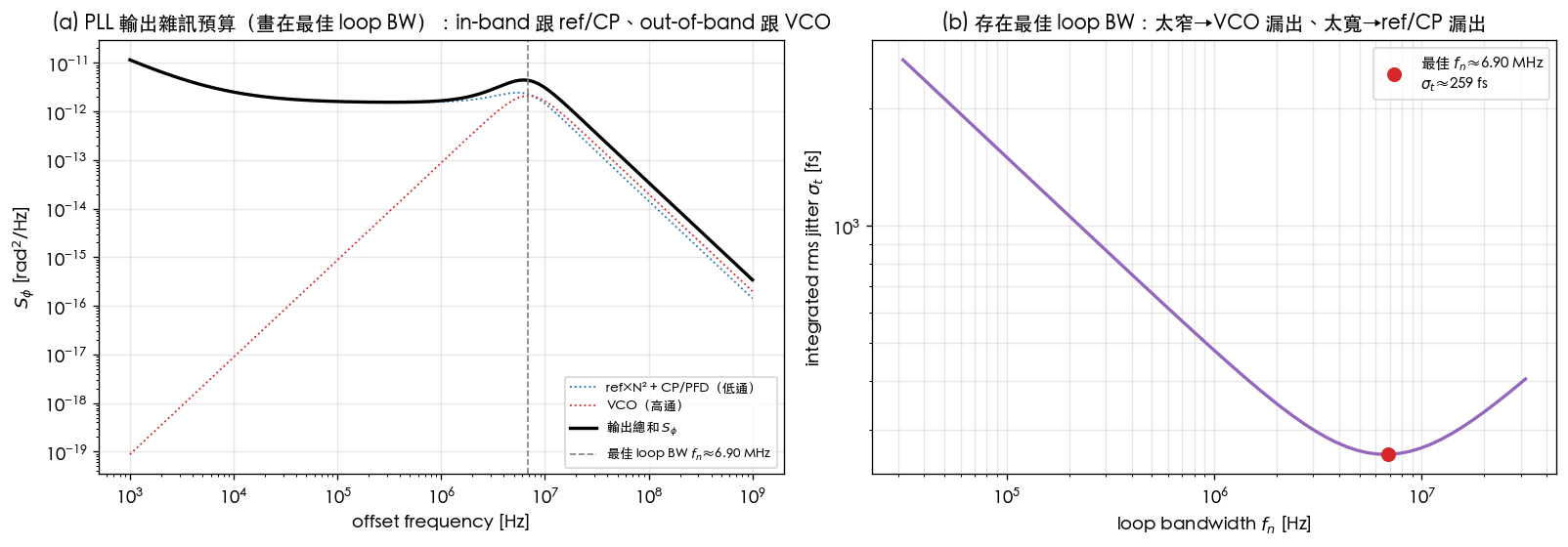
Corresponding simulation figure (lab_20)
lab_20 (simulations/lab_20_pll_budget.py) uses the type-II second-order budget above. The
left panel, at fixed MHz, plots three curves (ref+CP low-pass, VCO
high-pass, and the sum); the right panel sweeps and plots as a U-shape,
marking its minimum.
Parameter table (lab_20, representative levels, not a specific silicon process, illustrative):
| Quantity | Value | Description |
|---|---|---|
| 5 GHz | VCO/output frequency | |
| 100 | division ratio (reference dB amplification) | |
| 0.707 | damping ratio (near critical, small peaking) | |
| clean crystal: low flat floor + slight | ||
| (flat) | combined PFD/charge-pump/divider in-band floor | |
| ring VCO, dBc/Hz @ 1 MHz, | ||
| Integration range | – Hz | 1 kHz to 1 GHz |
Units table:
| Quantity | Unit |
|---|---|
| Hz | |
| rad/s | |
| dimensionless | |
| rad | |
| s |
How to read the figure:
- Left panel: the blue dotted curve (ref+CP) is a flat floor at in-band (), pulled down by the low-pass beyond ; the red dotted curve (VCO high-pass) is suppressed in-band and leaks out along out-of-band; the black curve (the sum) = flat close-in, following the VCO's far-out, with the crossover near and a slight peaking.
- Right panel: vs. is U-shaped. too narrow (left arm) → too much VCO close-in leaks through → jitter blows up; too wide (right arm) → too much ref/CP carried through → jitter rises again. The minimum lands at MHz, fs (lab_20's measured printed values).
Core Python (full script: simulations/lab_20_pll_budget.py):
import numpy as np
from simulations.common.pll_utils import H_lowpass_mag2, H_highpass_mag2

def output_psd(f, fn, N, zeta=0.707):
    lp = H_lowpass_mag2(f, fn, zeta)
    hp = H_highpass_mag2(f, fn, zeta)
    S_ref = 1e-16 + 1e-18 * (1e6 / f)   # clean crystal
    S_cp  = 5e-13 * np.ones_like(f)     # PFD/CP/divider flat floor
    S_vco = 2e-10 * (1e6 / f) ** 2      # ring VCO -100 dBc/Hz @1MHz, 1/f^2
    return (S_ref * N**2 + S_cp) * lp + S_vco * hp   # budget sum

f = np.logspace(3, 9, 3000); f0 = 5e9; N = 100
fns = np.logspace(4.5, 7.5, 60)
jit = [np.sqrt(np.trapezoid(output_psd(f, fn, N), f)) / (2*np.pi*f0) for fn in fns]
k = int(np.argmin(jit))
print(fns[k]/1e6, "MHz", jit[k]*1e15, "fs")   # -> ~6.90 MHz, ~259 fs
Worked examples
Format: problem → step-by-step substitution (with units) → result → dimension check → one line of Python verification. Uses lab_20's representative values throughout ( GHz, , , the three 's from the table above).
Example 1 (in-band floor + the cost of the reference's ): find the deep in-band () output phase-noise floor, convert it to dBc/Hz, and compare how much difference (in dB) it makes if drops from 100 to 10.
Step by step:
- Deep in-band, , ; take the flat part (ignoring the reference's ):
- Compute the reference term: .
- Add the CP term: .
- Convert to dBc/Hz (, canonical Eq. 16): .
Result: the in-band floor , i.e. dBc/Hz. Of this, the reference contributes and the CP contributes — the reference is the dominant player in-band. If drops from 100 to 10, the reference term drops from to (a drop of dB), and in-band is now dominated by , with the total floor — an improvement of about dB.
Dimension check: — confirmed; taking reads as dBc/Hz — confirmed.
import numpy as np
S_ref, N, S_cp = 1e-16, 100, 5e-13
S_in = S_ref*N**2 + S_cp
print(S_in, "rad^2/Hz", round(10*np.log10(0.5*S_in), 1), "dBc/Hz")  # 1.5e-12, -121.2
print("N=10:", round(10*np.log10(0.5*(S_ref*10**2 + S_cp)), 1), "dBc/Hz")  # -125.9
Example 2 (the U-shape and optimal BW: narrow, optimal, wide — three points compared): using lab_20's complete budget, numerically integrate from 1 kHz–1 GHz, and compare the rms jitter at MHz (too narrow), MHz (optimal), and MHz (too wide), to verify the U-shape and its minimum.
Steps (concept + numerics):
- For each , compute frequency by frequency.
- Integrate to get (trapezoid rule), then take the square root to get .
- Convert to , with GHz.
Result (lab_20 numerics):
| What leaks through | ||
|---|---|---|
| 0.30 MHz (too narrow) | fs | large VCO close-in leakage (U-shape's left arm) |
| 6.90 MHz (optimal) | fs | balanced on both sides, the minimum |
| 30 MHz (too wide) | fs | ref/CP carried through (U-shape's right arm) |
Moving from the optimum toward narrow ( MHz), jitter rises to ; moving toward wide ( MHz), it rises to . The U-shape's left arm is steeper than the right — because this is a ring VCO ( large, its leakage very sensitive to BW), so "better to open it a bit wide than too narrow." This is exactly the design rule behind ring-PLLs' preference for large loop BW.
Dimension check: : → ; : — confirmed.
import numpy as np
from simulations.common.pll_utils import H_lowpass_mag2, H_highpass_mag2
f = np.logspace(3, 9, 3000); f0 = 5e9; N = 100
def Sout(fn):
    lp, hp = H_lowpass_mag2(f, fn), H_highpass_mag2(f, fn)
    S_ref = 1e-16 + 1e-18*(1e6/f); S_cp = 5e-13; S_vco = 2e-10*(1e6/f)**2
    return (S_ref*N**2 + S_cp)*lp + S_vco*hp
for fn in [0.3e6, 6.9e6, 30e6]:
    st = np.sqrt(np.trapezoid(Sout(fn), f))/(2*np.pi*f0)
    print(f"fn={fn/1e6:5.2f} MHz -> sigma_t={st*1e15:.0f} fs")  # 867 / 259 / 396 fs
The third term for fractional-N: ΔΣ quantization noise
The budget so far is integer-N: , so the frequency step can only be an integer multiple of . For fine steps (e.g. a 200-kHz channel spacing) without sacrificing , you need fractional-N (fractional division): dither the modulus between integers (÷ this reference period, ÷ the next, …) so the average modulus is (). This pays a double dividend — can be raised and shrinks, so the in-band floor drops directly — but the modulus dithering is itself a quantization error and becomes a new noise source. Generating the modulus sequence with a ΔΣ modulator (delta-sigma modulator — a feedback quantizer that shapes the quantization error toward high frequencies) pushes the error power out to high offsets where the loop's low-pass filters it away. This section writes it up as the budget's third term.
The shaped result in this section belongs to standard ΔΣ frequency-synthesis theory (external literature, not among this site's five source PDFs); the classic source: T. A. D. Riley, M. A. Copeland, and T. A. Kwasniewski, "Delta-Sigma Modulation in Fractional-N Frequency Synthesis," IEEE J. Solid-State Circuits, vol. 28, no. 5, pp. 553–559, May 1993. The derivation below is self-contained, step by step.
From modulus dithering to phase noise (four steps)
(i) The MASH-m output. An -th-order MASH (MASH-1-1-1 means : three cascaded first-order accumulators) produces the modulus-control sequence
where is the last stage's quantization error, modeled as white: uniformly distributed over , variance , with LSB (note: this is the quantization step 1 VCO cycle per reference period — not the of the offset ). The is the ΔΣ noise shaping: it pushes the error power toward high frequencies.
(ii) The error accumulates into phase (one integration). In reference period the divider swallows extra VCO cycles; each cycle is rad of output phase, and phase is the accumulation of frequency error:
(Accumulation is in the -domain, which eats exactly one order of shaping: -th-order frequency shaping → -th-order phase shaping.)
(iii) PSD of the white sequence. A white sequence at sampling rate spreads its power uniformly over (two-sided bookkeeping) → density per Hz; the discrete difference has magnitude response . Putting it together (referred to the output phase, before the loop):
( in , single-sided). Factor-of-2 bookkeeping flag (flagged every time): the literature's customary version is two-sided bookkeeping, which numerically happens to equal the SSB (because the in cancels the of single-siding); this site's strict single-sided convention needs the (giving ). Both notations appear in the literature — always state which one you are reading. This is the same class of factor-of-2 issue as [P1] Eq.(21)'s /4 (SSB bookkeeping) vs the clean time-domain /2.
(iv) No ! This term enters the loop at the PFD like and is low-passed by the same , but it is not multiplied by : the error is counted in "VCO cycles" to begin with, so the is already rad of output phase. If you insist on referring it to the divider output (only rad per cycle), you must multiply by (power ) to get back to the output — the cancels exactly. The most common rookie budget mistake is multiplying this term by anyway.
Dimension check: [rad²] ( is a dimensionless cycle count) [1/Hz] shaping factor [dimensionless] — checks out.
Into the budget: the third term
It shares the CP noise's path (low-pass) but has a completely different shape: for , , so
— a rising ramp of dB/dec (MASH-1-1-1: dB/dec), capping out at (shaping factor at most , i.e. dB). It is not a floor — it is a wall climbing up from low frequency; the loop must chop it with before the wall climbs high enough to hurt.
The two suppression knobs (why higher and narrower BW work):
- Raise : at fixed , — doubling drops it by dB (). Intuition: the total quantization power is fixed but spread over a wider Nyquist bandwidth, and the in the shaping denominator grows.
- Narrow the loop BW: the in-band spot value doesn't change (), but the low-pass intercepts the ramp earlier — the third term's peak lands near with magnitude (: halving drops the peak 12 dB); a brick-wall estimate of its integrated power scales as ( — extremely sensitive to BW). This pushes in the same direction as the U-shape's right arm ("narrow BW suppresses in-band"), but directly conflicts with a ring VCO's need for wide BW — fractional-N + a noisy VCO is the hardest budget combination, and one reason low-noise fractional-N synthesizers prefer LC VCOs.
Honest toy-model warning (important): this page's type-II second-order only falls dB/dec beyond — it cannot catch the dB/dec rise of . So in this toy model the third term keeps climbing at a net dB/dec past until the caps: with kHz the peak is dBc/Hz at MHz, about 22 dB above the VCO term at the same offset ( dBc/Hz). Real fractional-N loops therefore must add high-frequency loop-filter poles (third/ fourth-order loops) so the out-of-band rolloff beats dB/dec (external standard practice — see the Gardner and Razavi textbooks; not among this site's five source PDFs). This is the classic origin of "the third term looks harmless on paper, then a high-frequency hump pops up in silicon."
Worked example (Example 3: the MASH-1-1-1 spot contribution)
Example 3: MASH-1-1-1 (), MHz, , . Find at MHz (first without the loop, then through with MHz and 100 kHz respectively), and compare against this page's in-band floor of dBc/Hz.
Step by step:
- Prefactor: .
- Shaping factor: ; raised to the → (dimensionless).
- Before the loop: → dBc/Hz.
- MHz: ( dB) → dBc/Hz — 15 dB above the dBc/Hz floor; the in-band budget is wrecked: the BW is too wide, the ramp has already climbed to its top at 1 MHz and gets a boost from the peaking.
- kHz: ( dB) → dBc/Hz — pushed 3.6 dB below the floor, safe on a spot basis (but the high-frequency hump still needs checking — see the toy-model warning above).
- Alternatively, leave the BW alone and raise to 100 MHz: before the loop it becomes dBc/Hz, a 15.04-dB improvement (theoretical asymptote dB — checks out).
Dimension check: dimensionless ; after it reads as dBc/Hz — checks out.
import numpy as np
from simulations.common.pll_utils import H_lowpass_mag2

fref, m, Delta, f = 50e6, 3, 1.0, 1e6
P = (2*np.pi*Delta)**2/(12*fref)
shape = (2*np.sin(np.pi*f/fref))**(2*(m - 1))
raw = P*shape
print(f"{P:.4e}", f"{shape:.4e}", round(10*np.log10(raw), 2))
# -> 6.5797e-08 2.4871e-04 -107.86 (prefactor rad^2/Hz, shaping factor, before-loop dBc/Hz)
for fn in (1e6, 1e5):
    lp = H_lowpass_mag2(np.array([f]), fn, 0.707)[0]
    print(round(fn/1e3), round(10*np.log10(raw*lp), 2))
# -> 1000 -106.1, 100 -124.83 (L_dSigma(1 MHz) for fn=1 MHz vs 100 kHz, dBc/Hz)
raw2 = (2*np.pi*Delta)**2/(12*100e6)*(2*np.sin(np.pi*f/100e6))**(2*(m - 1))
print(round(10*np.log10(raw/raw2), 2))
# -> 15.04 (improvement in dB for f_ref 50→100 MHz; asymptote (2m-1)x3.01=15.05)

fs = np.logspace(3, np.log10(25e6), 200_000)
LdS = P*(2*np.sin(np.pi*fs/fref))**(2*(m - 1))*H_lowpass_mag2(fs, 1e5, 0.707)
k = int(np.argmax(LdS))
print(round(10*np.log10(LdS[k]), 2), round(fs[k]/1e6, 2))
# -> -103.6 18.55 (the third term's high-frequency hump under the toy 2nd-order loop: dBc/Hz, MHz)
Conditions of validity and failure (the ΔΣ white-noise model)
| Condition | Holds when | Fails when |
|---|---|---|
| white, uniform | is "busy" (no short limit cycle) or dithered | a simple fraction (e.g. ) → periodic pattern → fractional spurs (discrete spikes, not a continuous spectrum) |
| PFD/CP linear | high-frequency shaped noise gets filtered by the loop | CP up/down mismatch, nonlinearity → high-frequency noise folds back in-band (noise folding); silicon measures worse than the formula |
| loop rolloff beats the ramp | integral under control, no hump | a 2nd-order loop's dB/dec is not enough for (this section's toy demonstrated the dBc/Hz hump) |
| quantization error dominant | the formula above is the third term | DTC-assisted, digital PLLs and other fractional techniques have their own residuals (external literature) |
Design-knobs list
| Knob | Effect | How to tune |
|---|---|---|
| loop BW | U-shape minimum; in/out crossover | ; VCO noisy → open it wider |
| division ratio | in-band floor | lower (higher-frequency reference, fractional-N) to suppress in-band; but must manage fractional spurs |
| charge-pump current noise | in-band flat floor | increase CP current, reduce mismatch; too much costs power |
| damping ratio | peaking near | – suppresses the bump; too small is underdamped and peaky |
| VCO | how high is (the ISF!) | increase swing , reduce (LC instead of ring) → can relax |
| reference | close-in tilt | choose a low- crystal; a narrow BW can't suppress the ref once it's amplified by |
| CP current mismatch | reference spur | trim/calibrate the charge-pump; a narrow BW attenuates the spur but hurts VCO suppression |
| ΔΣ order , (fractional-N) | third-term ramp dB/dec, magnitude | doubling gives dB (); narrowing chops the ramp; add loop-filter poles to kill the high-frequency hump |
Connection to SerDes
The PLL output's (this page's right-panel minimum, fs) is exactly the jitter budget fed to a high-speed serializer/deserializer (SerDes)'s sampling clock. In serdes_clocking_connection, this directly determines the eye diagram's horizontal closure and BER (bit error rate): the shorter the UI (unit interval, i.e. the higher the data rate), the larger the fraction of the eye width the same eats up. So choosing the right loop BW to minimize PLL jitter is the source of the entire SerDes link's budget. The CDR (clock-data recovery) itself is also a PLL, and its jitter-tolerance transfer for input jitter is exactly this page's (low-frequency jitter can be tracked → tolerated, high-frequency → relies on eye margin), see lab_13_pll_cdr_transfer.
Conditions of validity and failure
| Condition | Holds when | Fails when |
|---|---|---|
| sources uncorrelated | powers add directly (this page's sum formula) | if CP and divider are correlated, cross terms are needed |
| linear PLL (small phase error) | type-II second-order closed loop is valid | large unlock/slew → nonlinear, transfer function no longer holds |
| VCO is (white-noise upconversion) | , this page's U-shape | with flicker ( close-in) present → optimal BW shifts, re-integration needed |
| ignoring loop-filter and spur | toy budget is adequate | precise design must include , reference spur, fractional spurs |
| integer-N | reference | fractional-N: ΔΣ quantization-noise third term (now covered in this page's "The third term for fractional-N" section) |
Key takeaways
- PLL output budget: (canonical 11.2).
- In-band tracks ref/CP (amplified by , low-passed), out-of-band tracks VCO (high-passed, leakage), with the crossover at .
- The VCO term is exactly this site's ISF result .
- The reference spur is a discrete spike (the ripple from CP mismatch/leakage), suppressed by a narrow BW but at the cost of VCO suppression.
- Optimal loop BW: minimize , ; too narrow leaks VCO, too wide leaks ref/CP. lab_20 numerics: MHz, fs.
- This ring-PLL's U-shape has a steeper left arm than right → favors a somewhat larger loop BW.
- A type-II with a zero always peaks: , , ; dB @ (the peak is exactly the golden ratio ). In a cascade the peak dBs add → the 0.1-dB telecom spec (needs ): single-loop optimal cascade optimal.
- The fractional-N third term: (SSB reading; this site's single-sided needs ), no , climbing at dB/dec (); doubling gives dB, a narrow BW chops the ramp; a 2nd-order loop cannot contain the high-frequency hump (add filter poles).
Further reading
- Derivation of the two transfer functions and jitter transfer: lab_13_pll_cdr_transfer
- Where the VCO term comes from (ISF→): white_noise_to_phase_noise
- Why ring's is high and LC's is low: lc_vs_ring
- Feeding into eye/BER: serdes_clocking_connection
- The budget's simulation script:
simulations/lab_20_pll_budget.py - The classic source for fractional-N ΔΣ shaping: T. A. D. Riley, M. A. Copeland, and T. A. Kwasniewski, "Delta-Sigma Modulation in Fractional-N Frequency Synthesis," IEEE J. Solid-State Circuits, vol. 28, no. 5, pp. 553–559, May 1993 (external literature, not among this site's five source PDFs)
- Standard textbooks for type-II loops, the PM mapping, and jitter-peaking specs: F. M. Gardner, Phaselock Techniques, 3rd ed., Wiley, 2005; B. Razavi, Design of CMOS Phase-Locked Loops, Cambridge Univ. Press, 2020 (external literature, not among this site's five source PDFs)