β: This English translation is in beta — the Traditional-Chinese original is the authoritative version.
Clock-chain noise accounting: ×N, ÷N, PLL, buffer — a one-page lookup table
Prerequisites: psd_phase_noise_jitter (, , phase↔time conversion), pll_noise_budget ( and the five-source budget — this page reuses them directly, no re-derivation), white_noise_to_phase_noise (where the VCO's dBc/Hz comes from) | Next: serdes_clocking_connection, exercises
In a real system there is no such thing as "one oscillator, used directly": the reference crystal is multiplied up by a PLL, divided back down by dividers, and passes through several buffer stages before reaching the sampler. The system engineer's daily question is: given the source , what is at every node of the clock tree? What is the integrated jitter of the final clock? The good news: bookkeeping for the entire chain needs only four rules. This page derives each of the four rules step by step (no skipped steps, with units, with failure conditions), then strings them together in one complete worked chain, computed all the way to the end.
Physical intuition (conclusion first): only two kinds of things ever happen to phase along a clock chain — (1) Deterministic phase scaling: ×N multiplies phase by ( dB), ÷N divides phase by ( dB), a PLL applies ×N to the reference in-band and low-passes it, and high-passes the VCO. Scaling acts on the entire curve; the offset axis does not move. (2) Additive independent noise: the buffer's and divider's own noise floor, uncorrelated with the input phase, adds in power (never in dB). There is also one beautiful conserved quantity: under ideal ×N/÷N, the time jitter in seconds is exactly unchanged — what changes is only "what angular fraction of one period the same error in seconds occupies".
Step 0: the one-page lookup table (conclusions first, derivations below)
| Component | Phase relation | accounting | Main failure conditions |
|---|---|---|---|
| Ideal ×N multiplier | (entire curve shifted) | small-angle approximation ( grows), offset near | |
| Ideal ÷N divider | sampling foldover (offset near ), divider's own floor | ||
| Through a PLL (×N) | in-band follows ref, out-of-band follows VCO | the pure second-order loop's ref tail (computed in Step 6 of this page) | |
| buffer / divider floor | correlated noise (shared supply/bias) cannot simply be power-added |
Convention statement (factor-of-2 discipline, consistent throughout this page): every on this page is SSB (single-sideband) dBc/Hz,
converted from via the small-angle approximation (canonical formula 16; noise_utils uses the same convention).
The worked chain's VCO anchor of dBc/Hz @ 1 MHz is the site's canonical example B, using the
"/4" SSB accounting of [P1] Eq.(21), p.185; the clean time-domain derivation's "/2" version gives (the famous 3 dB convention dispute, see
white_noise_to_phase_noise). The four rules on this page
(, power addition) are themselves ratio operations: as long as input and output use the same convention, /2 or /4 cancels,
and the rules' numbers are convention-independent — which is why the accounting rules can safely be used as a lookup table.
Rule 1: ideal ×N multiplication — why it is
Step 1 (write the signal as a function of phase). Using the decomposition of [P1] Eq.(1), p.181, take a sinusoidal waveform:
is the total phase (rad), is the excess phase (rad), (rad/s).
Step 2 (ideal multiplier = memoryless nonlinearity + bandpass). Any memoryless nonlinearity acting on : because is a -periodic function of , it can be expanded as a Fourier series in :
The key is the argument: every term is "an integer multiple of the instantaneous total phase, " — a memoryless element has no notion of time, it can only act on "the phase right now", so the excess phase is carried along completely intact.
Step 3 (bandpass selects the -th harmonic). A bandpass filter centered at picks the term:
This identity holds instant by instant — every frequency component of is multiplied by , with no frequency selectivity whatsoever.
Step 4 (convert to PSD and dB). Phase multiplied by (amplitude), power spectral density multiplied by :
The second equation used — input and output use the same convention, the cancels, so is independent of the /2-vs-/4 convention. For , dB dB.
- Physical meaning: multiplication creates no noise. It magnifies "the same absolute time jitter" into an -times larger angle — one output period is only as long as the input's, so the same error in seconds occupies times the fraction of an output period.
- The offset axis does not move (common mistake): what gets multiplied by is the phase amplitude, not the rhythm of the phase fluctuations. The entire curve shifts vertically up by ; the horizontal axis (offset ) is completely unchanged.
- Dimension check: dimensionless, in rad, in rad²/Hz, in dB ✓.
- Time-jitter conservation: — the edge error in seconds is unchanged (verified numerically in Step 5 below).
Failure conditions: (1) small-angle approximation — ; for large (e.g. , dB) it can approach 1 rad, collapses, and the carrier energy redistributes into a Lorentzian (the linewidth diffusion constant is magnified by , see lorentzian_linewidth); (2) sideband overlap — for offsets near the skirts of the harmonics mix into the bandpass; (3) real multipliers have their own additive floor (Rule 4).
ILCM addendum: this rule assumes a "memoryless nonlinearity + bandpass" — that kind of multiplier creates no noise; it just scales the input's excess phase by , unchanged. A real injection-locked clock multiplier (ILCM) is not that machine: it is a locked oscillator, so the carrier path is still deterministically (in-band reference noise still eats , , consistent with this rule) — but its own free-running phase noise is high-pass shaped by a first-order discrete-time loop (corner , where is the realignment factor per reference pulse), replacing this rule's "clean constant shift" assumption. Past the corner, the output noise is set by the ILCM's own oscillator quality — no longer something describes. Full derivation: subharmonic_injection.
Rule 2: ideal ÷N division — the rigorous origin of
The quadrature_and_coupled_oscillators page, in the ÷2-generates-I/Q section, directly cites ; this is the rigorous derivation's home for that equation, and the two pages' numbers agree (÷2 is dB).
Step 1 (timing of the input edges). The -th input rising zero crossing is defined by the total phase: . Substituting and solving:
The second equation used " slowly varying" (offset ) to replace with . Dimension check: ✓.
Step 2 (a divider only drops edges, never moves them). An ideal ÷N is an edge-picking machine: for every input edges it outputs one, and the output edge's time is exactly the time of the selected input edge. So the absolute time error passes to the output completely intact:
Step 3 (fold the time error back into the output carrier's phase). The output carrier is . The output excess phase follows from the same phase definition in reverse (, ):
Step 4 (PSD and dB).
÷2 is dB. Physical meaning: the same jitter in seconds, spread over a period times longer, is an angle times smaller. Perfectly symmetric with Rule 1: ×N then ÷N brings back to where it started, and (seconds) is unchanged throughout.
Failure conditions (both matter):
- Sampling foldover (aliasing): is defined only at the output edge instants — this is a system sampled at . Components of the input phase noise at offsets above fold back into the output band; for a flat wideband noise floor, division does not earn the full (foldover stacks the power back). The clean holds only for close-in noise at offsets . (External literature, not among the five source PDFs; for the standard divider noise model see Egan at the end of this page.)
- The divider's own floor: real dividers (CML latch, TSPC) have their own additive floor (Rule 4), often higher than "the cleanly divided-down signal" — after division the output can never be better than the divider's own floor.
Relation to [P4]: an injection-locked frequency divider (ILFD) uses the ISF's 2nd harmonic to lock to , implementing ÷2 ([P4], frequency division in Part II, see paper_004). The ÷N phase accounting () holds equally for the ILFD's carrier path; but an ILFD near the edge of its lock range has its own noise behavior, outside this page's ideal accounting.
Rule 3: through a PLL — the reference goes "×N + lowpass", the VCO goes "highpass"
A PLL is the closed-loop implementation of Rule 1: the divider brings the output back to for phase comparison, which forces "output phase reference phase" — so reference noise first takes (Rule 1), and is then shaped by the closed-loop lowpass ; the VCO's own noise is shaped by the highpass :
The two transfer functions (type-II second order, ) and the full five-source budget were derived step by step and verified in pll_noise_budget; this page reuses them directly without re-deriving (that page also includes the charge-pump floor ; to keep this page's worked chain focused on the four rules, the CP floor is folded conceptually into the "in-band floor" and omitted numerically, marked illustrative). The brick-wall accounting used for the lookup table is its asymptotic version:
- in-band (): , ⇒ .
- out-of-band (): , ⇒ (the free-running VCO skirt).
- Take the crossover at the loop bandwidth .
Dimension check: all in rad²/Hz, and dimensionless ✓. The brick-wall version is convenient but has one famous trap — the pure second-order loop's reference tail, laid out numerically in Step 6.
Rule 4: the buffer/divider additive floor — power addition, never dB addition
Step 1 (why a buffer is "additive"). A buffer regenerates edges: at the instant the input waveform crosses the switching threshold, the noise voltage (V) of the buffer's internal devices sits on top of the threshold and displaces the output edge by
( = slew rate at the threshold crossing, V/s. This is the same physics as waveform_slope's "most sensitive where the slope is small".) comes from the buffer's own devices and is uncorrelated with the input clock's phase.
Step 2 (uncorrelated ⇒ PSDs add). In phase this is pure addition:
(The cross term .) Converting to dBc/Hz gives the lookup-table formula — note you must convert to linear first, add, then convert back to dB:
Both are SSB on the same carrier with the same convention; the of cancels on both sides — so accounting directly in is legitimate, independent of the /2-vs-/4 convention.
Step 3 (multiplicative vs additive — the most important classification on this page). Rules 1–3 are multiplicative: they scale/shape the incoming phase curve as a whole; a clean source gives a clean output. Rule 4 is additive: the buffer injects new, independent noise, and the output can never be better than the buffer's own floor — however clean the source, one noisy buffer stage ruins it. That is what "floor dominates" means.
Step 4 (when the floor takes over — the dB-addition table). Let the signal sit dB above the floor; the penalty is :
| Output above by | Who dominates | |
|---|---|---|
| dB (signal much higher) | dB | floor completely invisible |
| dB | dB | floor starting to show |
| dB | dB | — |
| dB | dB | — |
| dB (equal) | dB | half and half |
| dB (signal below floor) | output | floor dominates, output is clamped |
Step 5 (flat floor ⇒ white phase noise ⇒ one easy-to-remember jitter formula). A flat is white phase noise; its own rms jitter contribution over an integration bandwidth (Hz):
(The is the small-angle conversion, canonical formula 16; then integrate with canonical formula 19.) Numbers: dBc/Hz, MHz, GHz: fs. Dimension check: , ✓. (This 16.0 fs will reappear, unchanged, in the worked chain's breakdown below.)
The four rules' constants are first pinned down with a checkable Python block (the values after # -> are actual run output):
import numpy as np
print(round(20*np.log10(50), 2))   # -> 33.98
print(round(20*np.log10(2), 2))    # -> 6.02
print(round(10*np.log10(1 + 10**(-20/10)), 2))  # -> 0.04
print(round(10*np.log10(1 + 10**(-10/10)), 2))  # -> 0.41
print(round(10*np.log10(1 + 10**(-6/10)), 2))   # -> 0.97
print(round(10*np.log10(1 + 10**(-3/10)), 2))   # -> 1.76
print(round(10*np.log10(1 + 10**(0/10)), 2))    # -> 3.01
Step 5: the conserved quantity — under ideal ×N/÷N, (seconds) is unchanged
Put the conclusions of Rules 1 and 2 side by side: ×N gives while the carrier gets ; ÷N gives while . Substituting into (canonical formula 17), the two 's cancel:
Time jitter in seconds is the invariant of ideal multiplication/division. The that got worse (or better) is only a change in the exchange rate "the same error in seconds converted to angle". This gives you an extremely useful sanity check: on any chain segment that is "pure ×N/÷N with no additive floor", the computed at both ends over the same integration band must be equal. Verify with the worked chain's numbers (the 5 GHz stage vs the 2.5 GHz after ideal ÷2, both without the buffer):
import numpy as np
from simulations.common.noise_utils import integrate_rms_jitter
f = np.logspace(4, 8, 20001)
L5G = np.where(f <= 1e6, -126.02, -148.0 - 20*np.log10(f/1e6))
st5, _ = integrate_rms_jitter(f, L5G, f0=5e9, fmin=1e4, fmax=1e8)
st25, _ = integrate_rms_jitter(f, L5G - 6.02, f0=2.5e9, fmin=1e4, fmax=1e8)
print(round(st5*1e15, 1))    # -> 22.5
print(round(st25*1e15, 1))   # -> 22.5
The two 22.5 fs values are identical — ÷2 improved by 6 dB yet saved not a single fs. For SerDes this is actually the flip side of bad news: converted to UI, is unchanged while the UI gets longer, so after division the "fraction of a UI" does shrink — what you save is a ratio, not seconds.
Step 6: worked chain — 100 MHz → ×50 PLL → 5 GHz → ÷2 → 2.5 GHz → buffer
Now string the four rules into a realistically shaped chain. All values are representative/illustrative (not a specific silicon process) but fully consistent with the site's canonical numbers.
Parameter table:
| Quantity | Value | Unit | Notes |
|---|---|---|---|
| 100 | MHz | reference frequency | |
| (flat floor) | dBc/Hz | far-out floor of a clean reference (illustrative; a real crystal's close-in tilts up, this page only looks at kHz) | |
| 50 | — | ||
| 1 MHz, 0.707 | Hz, — | type-II second-order loop (reused from pll_noise_budget) | |
| VCO | , | dBc/Hz | site canonical example B ([P1] Eq.(21), p.185, /4 SSB convention) |
| ÷N | 2 | — | GHz |
| (flat floor) | dBc/Hz | the output buffer's additive floor | |
| Integration band | – | Hz | final jitter integration |
6.1 Per-stage : 100 kHz for in-band, 10 MHz for out-of-band
Step-by-step hand calculation (brick-wall accounting):
- Reference: flat floor ⇒ at both offsets.
- PLL output (5 GHz):
- in-band (): Rule 3 ⇒ .
- out-of-band (): free-running VCO, extrapolated from the 1 MHz anchor: .
- ÷2 (2.5 GHz): Rule 2, entire curve dB ⇒ and .
- Output buffer: Rule 4, power-add against the floor:
- 100 kHz: signal is 22.96 dB above the floor ⇒ penalty dB ⇒ (floor invisible).
- 10 MHz: signal is 19 dB below the floor ⇒ floor dominates ⇒ (clamped near ).
| Node | Carrier | (100 kHz) [dBc/Hz] | (10 MHz) [dBc/Hz] | Dominant rule |
|---|---|---|---|---|
| Reference | 100 MHz | — | ||
| PLL ×50 output | 5 GHz | Rule 3 (in-band ref+34; out-of-band VCO) | ||
| After ÷2 | 2.5 GHz | Rule 2 () | ||
| + buffer (final) | 2.5 GHz | Rule 4 (floor dominates at 10 MHz) |
The same table pinned down with checkable Python:
import numpy as np
L_ref = -160.0
L_in = L_ref + 20*np.log10(50)               # Rule 1/3: in-band = ref + 20logN
print(round(L_in, 2))                        # -> -126.02
L_vco_10M = -148.0 - 20*np.log10(10e6/1e6)   # VCO 1/f²: extrapolate from the 1 MHz anchor to 10 MHz
print(round(L_vco_10M, 2))                   # -> -168.0
div = -20*np.log10(2)                        # Rule 2
print(round(L_in + div, 2))                  # -> -132.04
print(round(L_vco_10M + div, 2))             # -> -174.02
def padd(*Ls): return 10*np.log10(sum(10**(L/10) for L in Ls))
print(round(padd(L_in + div, -155.0), 2))    # -> -132.02
print(round(padd(L_vco_10M + div, -155.0), 2))  # -> -154.95
6.2 Integrated jitter of the final 2.5 GHz clock (10 kHz–100 MHz)
Brick-wall model of the final curve: in-band floor (up to MHz), then the ÷2'd VCO skirt (1 MHz anchor , ), all power-added with the buffer floor throughout. Hand-integrating with canonical formulas 18/19 ():
Dimension check: ✓;
✓. Verified with noise_utils (same convention ):
import numpy as np
from simulations.common.noise_utils import integrate_rms_jitter
f = np.logspace(4, 8, 20001)
L_core = np.where(f <= 1e6, -132.04, -154.02 - 20*np.log10(f/1e6))
L_tot = 10*np.log10(10**(L_core/10) + 10**(-155.0/10))
st, sp = integrate_rms_jitter(f, L_tot, f0=2.5e9, fmin=1e4, fmax=1e8)
print(round(st*1e15, 1))   # -> 27.6
print(round(sp*1e6, 1))    # -> 433.4
Who contributed these 27.6 fs? (breakdown from an actual run of simulations/fig_clock_chain.py, power ratios)
| Source | Standalone | Share of |
|---|---|---|
| in-band floor (reference ) | 22.4 fs | 65.9 % |
| buffer floor | 16.0 fs | 33.7 % |
| VCO skirt | 1.78 fs | 0.42 % |
| RSS total | 27.6 fs | 100 % |
This table is the most important design message on this page: this chain's jitter is split between "the in-band floor raised by " and "the unremarkable buffer floor"; that beautiful dBc/Hz VCO is nearly invisible (0.42 %). Spending effort improving the VCO further is wasted work — do the accounting first, so the effort goes where it counts. (The buffer's 16.0 fs is exactly the number from Rule 4's Step-5 formula.)
6.3 Corresponding simulation figure
Full script: simulations/fig_clock_chain.py (to run: from the project root,
PYTHONPATH=. python3 simulations/fig_clock_chain.py — it prints every # -> number on this page and produces the figure).
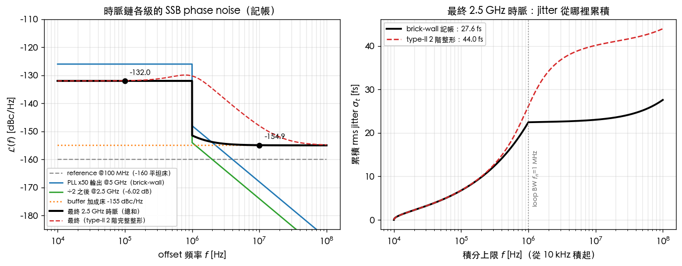
How to read it: in the left panel, the blue line is the 5 GHz brick-wall (in-band plateau + VCO skirt past 1 MHz), the green line is the same curve shifted down 6.02 dB (÷2), the orange dotted line is the buffer floor, and the thick black line is the final output — at 100 kHz, clamped by the floor at at 10 MHz. The right panel is the cumulative jitter "integrated from 10 kHz to ": the in-band floor accumulates 22 fs before 1 MHz, after which the buffer floor slowly pushes the total to 27.6 fs; the dashed red line (full type-II shaping) stays above the brick-wall around and beyond — that is the trap the next step lays open.
Step 7: honest comparison — brick-wall lookup vs full type-II shaping
Brick-wall is lookup-table-grade approximation. Computing with
pll_noise_budget's actual
(pll_utils, MHz, ), the difference at the two offsets is plain:
- in-band (100 kHz): shaped vs brick-wall — only 0.1 dB apart (slight peaking of at ). The lookup table is reliable ✓.
- out-of-band (10 MHz): shaped vs brick-wall — 7 dB apart!
The reason: the type-II second-order closed loop's zero makes roll off at only dB/dec for (), so the reference floor raised by leaks a dB/dec tail into the out-of-band region; and the VCO skirt is also dB/dec — the two lines are parallel, the gap is constant and can never be closed:
import numpy as np
from simulations.common.pll_utils import H_lowpass_mag2
S_refN2 = 2 * 10**(-126.02/10)          # N²·S_ref (S_phi of the in-band floor) [rad²/Hz]
lp = H_lowpass_mag2(10e6, 1e6)          # |H_lp|² @ 10 MHz, fn = 1 MHz
L_refpath = 10*np.log10(0.5 * S_refN2 * lp)
print(round(L_refpath, 1))              # -> -143.0
print(round(L_refpath - (-168.0), 1))   # -> 25.0
The reference tail at 10 MHz is dBc/Hz (5 GHz carrier), 25 dB above the VCO's —
and because both have the same slope, these 25 dB hold at every out-of-band offset. The lookup-table cell
"out-of-band = VCO" is, for a pure second-order loop, simply unreachable. The consequence for integrated jitter
(actual run of fig_clock_chain.py):
| Model | Final (10 kHz–100 MHz) |
|---|---|
| brick-wall lookup | 27.6 fs |
| type-II second-order full shaping | 44.0 fs () |
| second order + 3rd pole @ 3 MHz (illustrative) | 38.6 fs |
How to fix it: real synthesizers add a third pole to the loop filter (plus higher-order post-filters) precisely for this, turning the ref tail into dB/dec or steeper; the third row above shows one 3 MHz pole cutting the damage by a third (the pole-placement vs loop-stability trade-off belongs to the standard PLL literature — external literature, not among the five source PDFs).
One level more honest: this chain's MHz was never the jitter-optimal choice to begin with — the crossover of the in-band floor () and the VCO skirt sits at kHz, far below 1 MHz. Sweeping for this chain with pll_noise_budget's U-curve method (shaped model, 3rd pole tracking at ): the minimum is at kHz, fs. Lookup accounting (this page) tells you each stage's bill; loop optimization (that page) tells you how to change the bill — two different things, don't mix them.
Design-knobs checklist
| Knob | Which rule it acts on | How to turn it |
|---|---|---|
| Division ratio (reference frequency) | Rules 1/3: in-band floor | 65.9% of this chain's jitter power comes from ref; raising to lower is the most effective move |
| Buffer floor | Rule 4 | 33.7% comes from one floor stage; increase buffer current/slew () to push the floor down; the fewer stages the better |
| Where to place the ÷N | Rules 2 + 4 | ÷N only divides the noise "upstream of it"; only when placed after the noisy source do you enjoy , and downstream buffer floors still add at full value |
| Loop BW | Rule 3 | this chain's optimum is kHz (not 1 MHz); the 79.6 kHz crossover is the first-order intuition |
| Loop order (3rd pole) | Rule 3 | the pure second-order ref tail runs parallel to the VCO (a constant dB in this example); only higher-order poles let out-of-band truly hand over to the VCO |
| VCO | Rule 3's | this chain's VCO is only 0.42% — do the accounting before deciding to touch it (for ISF knobs see tank_swing, lc_vs_ring) |
Connection to SerDes
The final 2.5 GHz clock's fs feeds directly into serdes_clocking_connection's eye/BER machinery: if this clock drives a 5 Gb/s half-rate link (UI ps), the RJ overhead at BER (, site canonical) is ps UI — quite healthy; but note every extra buffer stage in the clock tree adds another Rule-4 floor (power addition) — in a high-fan-out tree the buffers alone can eat the whole budget. Accumulated jitter of the free-running segment ([P2] Eq.(8), p.792, ) is high-pass truncated once it enters the PLL/CDR loop — in this chain, "who free-runs and who is locked" determines which noise accumulates and which does not (Step 6 of that page).
Applicability and failure conditions
| Condition | When it holds | When it fails |
|---|---|---|
| Small-angle approximation ( rad) | and the lookup hold | after large- multiplication grows → Lorentzian redistribution (lorentzian_linewidth) |
| offset (×N), (÷N) | clean | sideband overlap / sampling foldover; a flat floor does not earn the full |
| Per-stage noise uncorrelated | Rule-4 power addition | correlated noise sharing supply/bias (e.g. PSIJ) needs the cross terms, may add in phase |
| Brick-wall PLL accounting | in-band lookup error dB | pure second-order loop: ref tail parallel to VCO (constant 25 dB gap in this example), the out-of-band cell can be off by 7 dB, underestimated by 59% |
| Ideal edge-picking divider | real divider's own floor (Rule 4) dominates first; ILFD near the lock-range edge is a separate story ([P4]) |
Key takeaways
- The four rules: ×N adds (, offset axis unchanged); ÷N subtracts (edge-picking, time error intact, angle divided by ); PLL = reference through , VCO through (transfer functions reused from pll_noise_budget); buffer/divider floor = power addition, .
- Conserved quantity: under ideal ×N/÷N, (seconds) is unchanged (both ends 22.5 fs in this example); ÷N saves "fraction of a UI", not seconds.
- Worked chain (100 MHz→×50→5 GHz→÷2→2.5 GHz→buffer): at 100 kHz, ; at 10 MHz, (floor dominates).
- Final integrated jitter (10 kHz–100 MHz) = 27.6 fs; breakdown = ref floor 65.9% + buffer floor 33.7% + VCO 0.42% — accounting first, don't blindly upgrade the VCO.
- Honest comparison: the pure type-II second-order loop's ref tail runs parallel to the VCO skirt (a constant dB here), shaped fs (59% above the lookup); adding a 3rd pole (3 MHz) → 38.6 fs; this chain's jitter-optimal loop BW is actually kHz ( fs).
- Convention discipline: the rules are all ratio/addition operations, /2-vs-/4 cancels; the only convention-sensitive item is the VCO anchor ( = [P1] Eq.(21)'s /4 SSB; the time-domain /2 gives ).
Further reading
- PLL transfer functions and the five-source budget (where this page's Rule 3 is fully derived): pll_noise_budget, lab_13_pll_cdr_transfer
- ÷2 quadrature generation and ILFD (cites this page's Rule 2): quadrature_and_coupled_oscillators, paper_004
- Connecting to eye/BER: serdes_clocking_connection
- Where the small-angle approximation goes after large- multiplication breaks it: lorentzian_linewidth
- Origin of the dBc/Hz VCO anchor and /2-vs-/4: white_noise_to_phase_noise
- This page's simulation script:
simulations/fig_clock_chain.py
External literature (not among the five downloaded PDFs)
- The of ×N/÷N, divider sampling foldover, additive floors: standard frequency-synthesis accounting (external literature, not among the five source PDFs; found in any frequency-synthesis textbook). Standard references: W. F. Egan, Frequency Synthesis by Phase Lock, 2nd ed., Wiley, New York, 2000; B. Razavi, RF Microelectronics, 2nd ed., Prentice Hall, Upper Saddle River, NJ, 2012.
- What the site's five PDFs provide is the physics of the chain's "sources": [P1] (the VCO's and the ISF), [P2] (the ring's accumulation), [P3]/[P4] (injection locking and the ILFD division mechanism).