β: This English translation is in beta — the Traditional-Chinese original is the authoritative version.
Lab 13 — PLL/CDR jitter transfer: VCO high-pass, reference low-pass
Breadcrumb: Simulation labs › System & advanced › This page (PLL/CDR jitter transfer). Upstream: lab_11; downstream: lab_12.
This lab explains something practically crucial: how a PLL (phase-locked loop) / CDR (clock and data recovery) "filters" an oscillator's phase noise. The key conclusion — referred to the output phase, the VCO's (voltage-controlled oscillator's) own phase noise is high-pass shaped (close-in suppressed, far-out dominant), while the reference clock's phase noise is low-pass shaped. This is why a noisy ring VCO, once locked to a clean reference, can still deliver a usable clock.
Physical intuition (conclusion first): a PLL is a negative-feedback loop that tracks the reference phase. Inside the loop bandwidth (low offset, slow variation), the feedback reacts in time, so the output follows the reference — the reference's low-frequency noise passes straight to the output (reference low-pass), while the VCO's own low-frequency drift gets corrected away by the feedback (VCO high-pass). Beyond (high offset, fast variation), the feedback cannot keep up and the output follows the VCO free-running — VCO noise passes through unchanged (the passband of the VCO high-pass) and the reference's high-frequency noise is filtered out (the stopband of the reference low-pass). The crossover sits at the loop bandwidth .
1. Learning objectives
- Understand the PLL's two phase-noise transfer functions: reference→output is a low-pass , VCO→output is a high-pass , with .
- Synthesize the locked output with .
- See that "close-in follows the reference, far-out follows the VCO, crossover at the loop bandwidth ".
- Connect to the design trade-off: how to choose the loop bandwidth so as to suppress VCO close-in without amplifying reference far-out.
2. Mathematical model
Closed-loop transfer functions of the type-II second-order PLL (spec section 10.2, "PLL (type-II 2nd order)"). Written in terms of the natural frequency and damping ratio , referred to the output phase:
where ( is the offset frequency).
- Limit check (low frequency ): (reference passes fully), (VCO suppressed). ✓ Matches "close-in follows the reference".
- Limit check (high frequency ): (reference filtered out), (VCO passes fully). ✓ Matches "far-out follows the VCO".
- Complementarity: with these standard forms one can verify (the same time-domain error shared between the two paths), so the output phase = the sum of the two.
- Dimension check: and are both rad/s; numerator and denominator are of the same order ( or ), so the transfer functions are dimensionless ✓.
Output phase noise (power superposition). The noise of the two paths is uncorrelated, so powers add (spec section 10.2):
- Dimension check: are all rad²/Hz, dimensionless, so the units of the sum are consistent ✓.
Representative input shapes for this lab (anchored, not a specific silicon process):
3. Block diagram
4. Core Python code
Verbatim from main() in simulations/lab_13_pll_cdr_transfer.py: set the loop bandwidth fn and damping zeta,
provide representative VCO and reference PSDs, then call shape_output_phase_noise to synthesize the output.
f = np.logspace(3, 9, 2000)  # 1 kHz .. 1 GHz offset
fn = 1e6  # loop natural frequency ~ 1 MHz
zeta = 0.707

# representative phase-noise PSDs (rad^2/Hz), anchored shapes
S_vco = 1e-6 * (1e6 / f) ** 2          # ring VCO: strong 1/f^2 close-in
S_ref = 1e-12 + 1e-14 * (1e6 / f) ** 2  # clean reference: low flat + slight 1/f^2

S_out, S_ref_sh, S_vco_sh = shape_output_phase_noise(f, S_ref, S_vco, fn, zeta)
The underlying transfer functions (pll_utils.py) are a verbatim implementation of the spec section 10.2 PLL formulas:
def H_lowpass_mag2(f, fn_hz, zeta=0.707):
    """|H_lp(j2*pi*f)|^2 for a type-II 2nd-order PLL (reference -> output)."""
    w = 2 * np.pi * np.asarray(f, dtype=float)
    wn = loop_natural_freq(fn_hz)
    num = (2 * zeta * wn * w) ** 2 + wn ** 4
    den = (wn ** 2 - w ** 2) ** 2 + (2 * zeta * wn * w) ** 2
    return num / den

def H_highpass_mag2(f, fn_hz, zeta=0.707):
    """|H_hp(j2*pi*f)|^2 = |1 - H_lp|^2 for the VCO -> output path."""
    w = 2 * np.pi * np.asarray(f, dtype=float)
    wn = loop_natural_freq(fn_hz)
    num = w ** 4
    den = (wn ** 2 - w ** 2) ** 2 + (2 * zeta * wn * w) ** 2
    return num / den
- Internally,
shape_output_phase_noiseis simplyS_ref*lp + S_vco*hp, returning the output and the two shaped components. zeta=0.707(Butterworth damping) gives a flat closed loop with no visible jitter peaking.
5. Full script path
simulations/lab_13_pll_cdr_transfer.py
(Dependencies: H_lowpass_mag2, H_highpass_mag2,
shape_output_phase_noise, loop_natural_freq from simulations/common/pll_utils.py; savefig from simulations/common/plot_utils.py.)
How to run: python scripts/run_all_sims.py.
6. Parameter table
| Parameter | Variable | Value | Notes |
|---|---|---|---|
| Offset sweep | f | Hz (logspace 2000) | 1 kHz–1 GHz |
| Loop natural frequency | fn | Hz | loop bandwidth crossover point |
| Damping ratio | zeta | Butterworth, no peaking | |
| VCO PN level | — | rad²/Hz | ring: strong |
| Reference PN level | — | rad²/Hz | clean: low flat + slight |
7. Units table
| Quantity | Symbol | Unit | Value in this lab |
|---|---|---|---|
| Offset frequency | Hz | 1 kHz–1 GHz | |
| Angular frequency | rad/s | — | |
| Loop natural frequency | rad/s | ||
| Damping ratio | — (dimensionless) | 0.707 | |
| Power transfer | — (dimensionless) | ||
| Phase PSD | rad²/Hz | see parameter table |
8. Simulation figure
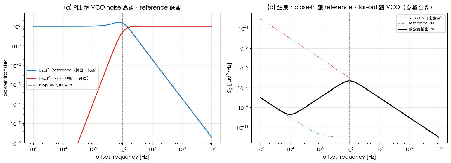
9. How to read the figure
- Left panel (transfer functions): the blue curve is 1 (0 dB) at low offsets and rolls off past (low-pass); the red curve approaches 0 at low offsets and rises to 1 past (high-pass). The two cross near MHz (gray dashed line) — that is the loop bandwidth.
- Right panel (output PN synthesis):
- The black curve (locked output) close-in () hugs the blue reference — the VCO's strong has been suppressed by the high-pass.
- Far-out () the black curve hugs the red VCO — the reference's high frequencies are low-pass filtered out and the VCO passes through unchanged.
- The crossover (where the two inputs are comparable) sits near .
- Core message: locking swaps "the noisy VCO's close-in" for "the clean reference's close-in", at the cost that far-out is still set by the VCO. The loop bandwidth is the design knob: raising → suppresses more VCO close-in but admits more reference far-out and possible jitter peaking; lowering does the opposite.
- CDR view: think of the "reference" as the jitter of the incoming data — a CDR low-pass tracks low-frequency input jitter (jitter tolerance) and high-pass rejects high frequencies — the same shaping.
10. Corresponding paper equations/figures
- PLL transfer functions: spec section 10.2, "PLL (type-II 2nd order)": , and . Generic PLL/CDR theory — external literature, not among the five source PDFs — supplemented from standard references.
- The VCO noise being shaped itself comes from the ISF phase noise of [P1]/[P2] (a ring VCO's corresponds to spec Eq. 21 and the ring discussion in [P2]); this lab feeds that into the loop shaping.
- Stopping jitter accumulation: echoes lab_11 — the free-running accumulation is exactly what the PLL's high-pass shaping reins in close-in.
- Corresponds to site figure
pll_cdr_jitter_transfer.png; for the design chain see serdes_clocking_connection.
11. Limitations and approximations
- This is a pedagogical toy model, not transistor-level: ideal type-II second-order closed-loop expressions; no charge-pump non-idealities, divider, loop-filter parasitics, reference spurs, etc.
- Linear, time-invariant, small-phase assumption: phase-domain linearization (the small-signal model of a locked PLL); large loss of lock and cycle slips are out of scope.
- Second-order approximation: real loops often contain extra poles (third order and above) affecting high-frequency roll-off and stability; only the dominant second-order behavior is kept here.
- Uncorrelated-noise assumption: requires the reference and VCO noise to be uncorrelated (powers add). In practice, shared bias/supply can correlate them.
- Input PSD shapes are illustrative: the levels and shapes of , are anchored examples, not measurements of a specific silicon process; the point is the shaping mechanism and the crossover at , not absolute dBc/Hz.
- No jitter-peaking detail: is deliberately chosen flat; a smaller produces peaking near (a bump in the output PN), a case this figure does not sweep.
Key takeaways
- Referred to the output phase: the reference is low-passed (), the VCO high-passed (), with .
- ; close-in follows the reference, far-out follows the VCO, crossover at the loop bandwidth .
- This is why a noisy ring VCO locked to a clean reference can still deliver a good clock.
- The loop bandwidth is the central knob: raising it suppresses VCO close-in but admits reference far-out and peaking risk.
Further reading
- Where the VCO's comes from: white_noise_to_phase_noise
- Why free-running accumulation demands locking: lab_11_monte_carlo_jitter
- How output jitter affects BER: lab_12_serdes_eye_ber
- Design chain: serdes_clocking_connection
- Use in design/theory: multiply each noise source by its transfer function, build the whole-PLL noise budget and the optimum loop BW → pll_noise_budget