β: This English translation is in beta — the Traditional-Chinese original is the authoritative version.
ISF in real topologies: cross-coupled LC VCO, Colpitts, CMOS ring stage
Prerequisites: effective_isf (cyclostationary effective ISF , the common skeleton for all three topologies on this page), symmetry ( sets ; why the tail's is the real trouble), waveform_slope (deriving the ring stage's ISF from switching slope) | Next: lc_vs_ring, measurement_and_spurs
The preceding pages all used the ideal-LC as the lead character to lay out the mechanism white noise → , flicker → . But a real oscillator on silicon is not a clean LC plus a single white-noise source — it is several transistors, a tail (bias) current source, a tank, plus switching action. Different devices inject their noise at different nodes and different phase windows, so every noise source "sees" a different effective ISF. This page answers:
What this page answers: in three of the most common topologies — the cross-coupled LC VCO, Colpitts, and the CMOS inverter ring stage — what does the ISF actually seen by each device-noise source look like? Where do its Fourier harmonics () land? And how do those harmonics set the close-in and ? We walk all of this by hand calculation plus order-of-magnitude estimation (not Spectre / not transistor-level netlist extraction), stringing device noise → ISF harmonics → close-in PN into one complete chain for each topology.
Physical intuition (conclusion first): the ISF is "the shape of phase sensitivity to charge injected at some node." But the noise source does not inject uniformly over the whole cycle — the tail transistor only conducts during the switching instant, the Colpitts transistor only conducts during one narrow current pulse, and a ring's inverter only carries large current during transition. Multiplying "how much noise the device injects, and in which phase window" (i.e., the cyclostationary noise modulating function ) by "that node's ISF " gives the effective ISF . The Fourier harmonics of this product — especially (which sets flicker upconversion to ) and (which folds noise near back onto the carrier) — are what actually drive real close-in phase noise.
This page uses two signature close-in formulas from [P1] (verified verbatim):
Flicker upconversion to ([P1] Eq.(23), p.185):
corner ([P1] Eq.(24), p.185):
The white-noise signature result ([P1] Eq.(21), p.185), used here to compute the floor:
The cyclostationary effective ISF ([P1] Eq.(27), p.186 — replace with , where is the noise modulating function, an amplitude-modulation function):
Wherever a numeric value is marked illustrative, it is a pedagogical constructed model (not extracted from a transistor netlist), whose purpose is to walk through the order of magnitude of a known mechanism; the ideal-LC is exact. The specific mechanism behind the tail's effective ISF comes from the Hajimiri–Lee cyclostationary analysis ([P1] §IV.D) and from Andreani et al.'s tail-noise analysis (external literature, not among the five source PDFs — see end of page).
(a) Cross-coupled LC VCO: clean tank, troublesome tail
Circuit and the two key noise sources
The skeleton of a cross-coupled LC VCO: an LC tank across the two differential nodes ; below it, a cross-coupled NMOS pair (, gates tied to each other's drains) supplies (negative conductance) to compensate tank loss; at the bottom, a tail current source sets the bias current .
Two fundamentally different noise-injection points:
- The differential tank nodes ('s channel thermal noise lands directly on the tank) → sees the tank's ISF.
- The tail node ('s thermal + flicker noise) → sees the tail's effective ISF, because the tail current must first be "commutated" by the switching pair before it reaches the tank.
Tank ISF: pure , a
The differential tank is a near-ideal LC resonator, with the two terminal voltages approximately . Injecting charge into the differential node gives the ideal-LC phase-sensitivity result (see impulse_to_phase_shift):
Its Fourier series has only one term, , with all other . .
- Physical meaning: is most sensitive at the zero crossings () and zero at the peaks () — the classic "a kick is most effective where the slope is steepest."
- Key benefit: . From [P1] Eq.(23), strength is proportional to ; means differential tank noise barely upconverts flicker at all. This is why a differential LC VCO's close-in phase noise is cleaner than a ring's — provided the waveform is symmetric so stays near 0.
The tail's effective ISF: rich in and
The story for tail noise is entirely different, because the tail node voltage swings at , and the switching pair applies full-wave-rectifier-like commutation to the tail current. Intuitively:
- On each half cycle, or alternately steers the entire (including its noise) to one side of the tank; over one full RF period the tail current is "flipped" twice → the tail sees a -periodic modulation → this naturally produces (second harmonic).
- The tail current's low-frequency/DC noise (especially flicker) gets averaged by switching into a common-mode swing, leaving a nonzero (DC term) — this is the gateway for flicker upconversion.
We write this shape down with an illustrative model (taken from lab_21_topology_isf.py, marked as a constructed model):
- : the DC term — the culprit behind flicker upconversion ([P1] Eq.(23) is proportional to ).
- : the second harmonic — folds tail thermal noise near back onto the carrier at offset .
- : a residual fundamental (should be 0 under ideal symmetry; asymmetry leaks a little through).
- This ISF's (Parseval; see figure caption).
Mechanism of the fold-back (hand-calc intuition): tail thermal noise carries power near . The ISF's term acts as a "mixer that down-converts at " (see white_noise_to_phase_noise, step 3a): it moves noise at to phase at offset . This is exactly why designers raise the tail current source's impedance at (a tail filter): placing an LC trap or a large capacitor at makes the tail node high-impedance (ideally open) at , so tail noise at can no longer inject into the tank → the fold-back is choked off.
Figure: tank vs. tail ISF and harmonics
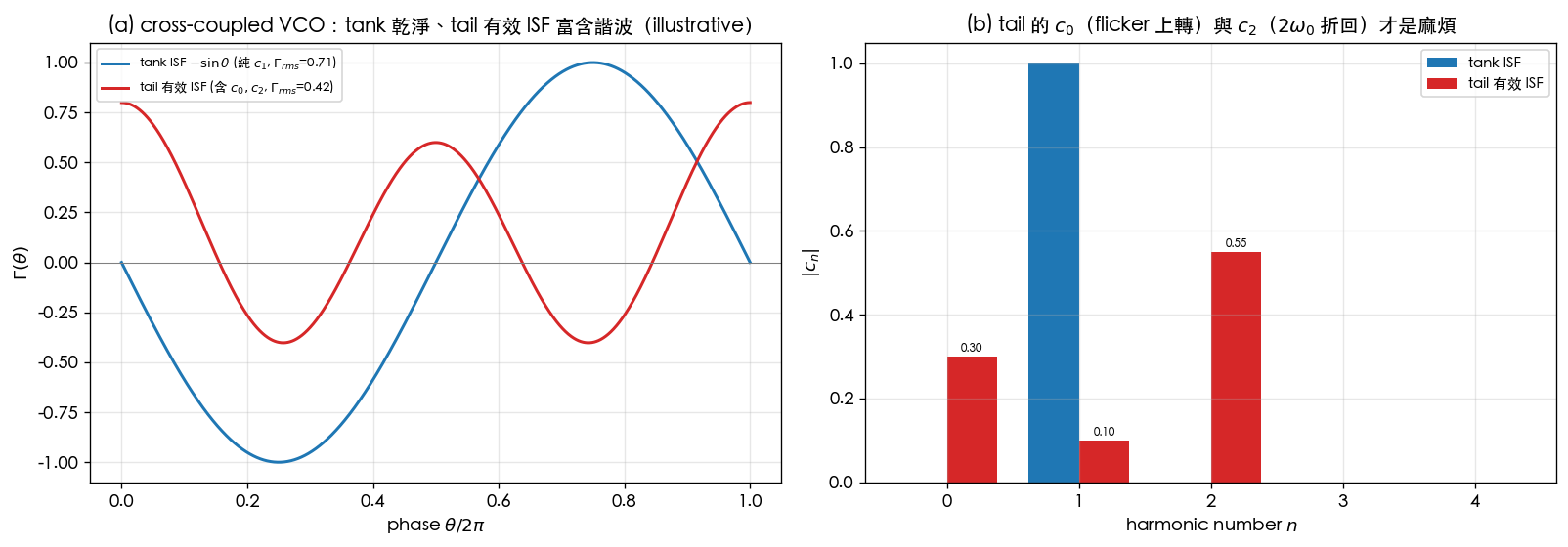
(Full script: simulations/lab_21_topology_isf.py, marked illustrative — the tank's is exact; the tail's values are a constructed pedagogical model used to demonstrate a known mechanism.)
| Item | Tank ISF | Tail effective ISF |
|---|---|---|
| Formula | ||
| Dominant harmonics | (pure fundamental) | , , |
| (illustrative) | ||
| Close-in risk | Almost no () | Large → strong ; large → fold-back |
| Countermeasure | Maintain waveform symmetry | Waveform symmetry lowers + tail filter tuned to lowers |
| Model | Exact (ideal LC) | Illustrative (constructed) |
Device noise → ISF harmonics → close-in PN: the tail's full chain (worked example 1)
Example 1 (tail flicker upconversion → corner, by hand): cross-coupled LC VCO, GHz, pC. The tail's effective ISF uses the illustrative model above (, ). Tail transistor white noise , flicker corner MHz ( rad/s). Find the corner , and compute at kHz (in the region).
Chain link 1 (device noise → ISF harmonics): the tail's noise sees the effective ISF with .
Chain link 2 ( corner, [P1] Eq.(24)):
- Meaning: the region extends to about 255 kHz offset — smaller than the device flicker corner (1 MHz) by a factor . This is exactly [P1]'s key design message — the corner is not the same as the device's corner; it can be substantially shrunk by waveform symmetry (suppressing ).
Chain link 3 (close-in , [P1] Eq.(23)): at kHz:
- rad/s, .
- .
- .
- .
- Linear value inside parentheses .
- .
Result: kHz; dBc/Hz (in the region).
Dimension check (the bracket in [P1] Eq.(23) must be dimensionless): carries ; carries ; is dimensionless. Multiplying gives → per-Hz ✓.
import numpy as np
c0, qmax, Si = 0.30, 1e-12, 2e-23
gamma_rms = 0.42
w1f = 2*np.pi*1e6
# 1/f^3 corner (Eq.24)
dw_corner = w1f * c0**2 / (2*gamma_rms**2)
print(round(dw_corner/(2*np.pi)/1e3, 1), "kHz")     # -> 255.1 kHz
# L at 10 kHz (Eq.23)
dw = 2*np.pi*1e4
L = 10*np.log10((c0**2/qmax**2) * (Si/(8*dw**2)) * (w1f/dw))
print(round(L, 1), "dBc/Hz")                          # -> -82.4 dBc/Hz
Design knobs (cross-coupled LC VCO):
- Waveform symmetry (matched rise/fall edges) → suppresses → directly shrinks the corner (Eq.(24) is proportional to ).
- Tail filter tuned to (an LC trap / large capacitor at the tail node) → makes the tail node high-impedance at → suppresses fold-back.
- Increase (tank swing) → suppresses both (Eq.(21)) and (Eq.(23)) simultaneously, via the denominator.
- Reduce tail flicker (large tail-device sizing, PMOS tail) → lowers the flicker portion of .
(b) Colpitts: why the ISF concentrates in a narrow phase window
Circuit and current pulse
The Colpitts oscillator forms positive feedback with a single transistor plus a capacitive divider () and a tank inductor. Its signature feature: the collector (drain) current is not sinusoidal but a series of narrow, large current pulses followed by a long "quiet" interval. This is exactly what [P1] Fig. 13 shows — the collector voltage and collector current of the Colpitts oscillator of Fig. 5(a): the current is "a short period of large current followed by a quiet interval" ([P1] §IV.D, p.186).
Key point: pulse timing vs. ISF shape
Two independent periodic functions are multiplied here:
- The tank's own ISF (the Colpitts tank is also near-sinusoidal), spread over the full cycle.
- The noise modulating function : the device only conducts — and only injects noise — during the current pulse, so is a narrow pulse concentrated at some phase .
The effective ISF is the product of the two ([P1] Eq.(27)):
Because is a narrow pulse, is also "windowed" down to a narrow phase interval around — this is the mathematical statement of "the Colpitts ISF concentrates in a narrow phase window (the current-pulse injection instant)," corresponding to [P1] Fig. 14 (which plots , , and together).
Why this is good news for Colpitts
[P1] §IV.D's key observation (quoted verbatim): "The surge of current occurs at the minimum of the voltage across the tank where the ISF is small." That is, the current pulse lands right at the tank voltage's minimum — and is relatively small there (away from the zero crossings, in the low-sensitivity region). A well-designed Colpitts aligns noise injection with the phase window where ISF is small, so even though the device noise is large at that instant, multiplying by a small keeps small; stays low → close-in phase noise is low.
This is one of the core reasons Colpitts phase noise is excellent: not because its devices are quieter, but because it aligns the noise-injection instant with the least phase-sensitive window. Compare [P1] §IV.D: the ring oscillator's misfortune is that "the device current is largest at transition (where the ISF is also largest)" — the two peaks overlap, so and cyclostationary effects offer no help — this is one reason ring phase noise is worse.
Device noise → ISF harmonics → close-in PN: Colpitts' full chain (worked example 2)
Example 2 (how a narrow window suppresses , order-of-magnitude by hand): Colpitts, tank ISF . The device current pulse width is about of the period (conduction angle ), centered on where the ISF is small (take the representative value of within the pulse window as ). Compare for "noise injected uniformly over the full cycle" versus "noise injected only in the narrow window."
Case A (stationary, uniform over the full cycle): ,
Case B (cyclostationary, narrow window): model as a window of width and height (normalized so the average noise power inside the window is unchanged), located where . Within the window , with mean square:
(This is an order-of-magnitude approximation: window height , window width ; after normalization, the average inside the window is taken as roughly the center value . An exact value would require numerical integration — here we take only the order of magnitude.)
Comparison: drops from to , an improvement of about dB ( dB).
Chain closure (→ close-in PN): ([P1] Eq.(21) with replaced by ), so aligning noise injection with a small-ISF window directly cuts close-in PN by about 7 dB — this is the order of magnitude of Colpitts' advantage.
- Dimension check: is dimensionless ( and are both dimensionless) ✓.
- Honesty note: and are order-of-magnitude estimates (not precise values extracted from a netlist); the goal is to demonstrate how "a narrow window aligned with small ISF" suppresses . See [P1] Fig. 14 for the exact curve.
import numpy as np
theta = np.linspace(0, 2*np.pi, 20000, endpoint=False)
gamma = -np.sin(theta)
# Case A: stationary
g2_A = np.mean(gamma**2)                       # ~0.5
# Case B: narrow window alpha aligned with small-ISF region (centered near theta_p ~ 1.5*pi, |Gamma|~0.3 region)
alpha = np.zeros_like(theta)
mask = (theta > 1.40*np.pi) & (theta < 1.50*np.pi)   # ~10% window
alpha[mask] = 1.0/0.05                          # normalized height
g2_B = np.mean((gamma*alpha)**2) * 0.05         # order of magnitude
print(round(g2_A,3), round(g2_B,3))             # ~0.5  vs  ~0.09 order of magnitude
print(round(10*np.log10(g2_A/0.09),1), "dB")    # ~7.4 dB improvement
Design knobs (Colpitts):
- Align the current pulse with the tank-voltage trough (where ISF is small) — shrink the conduction angle, adjust bias so the pulse lands in the small- phase window.
- Narrower pulse (smaller conduction angle) — the narrower the window, the better it avoids the large-ISF zero crossings.
- Unlike cross-coupled: Colpitts is single-ended, single-device, and has no tail-switching fold-back problem, but waveform asymmetry will make (still watch for flicker upconversion).
(c) CMOS inverter ring stage: deriving the ISF from switching slope
From transition slope to ISF shape
A ring oscillator is a chain of CMOS inverter stages in a loop. Each stage's output is "parked" at a rail ( or GND) most of the time, flipping rapidly only during the brief switching transition. Question: what does this stage's ISF look like?
Hand-calc reasoning (slope → sensitivity): phase sensitivity fundamentally measures "how far the phase is pushed by a kick at this phase." For a threshold-crossing digital stage, phase = when the edge crosses the threshold. A small charge injected at the node produces a voltage jump , which shifts the edge-crossing instant by
converting to phase via . Comparing with the operational ISF definition gives
- Intuition: a large (steep transition) → the edge instant is shifted very little → local is small; but the edge only exists during the transition — on the rail (), a charge kick just gets "reshaped" by the next stage's threshold and barely shifts the edge timing → on the rail.
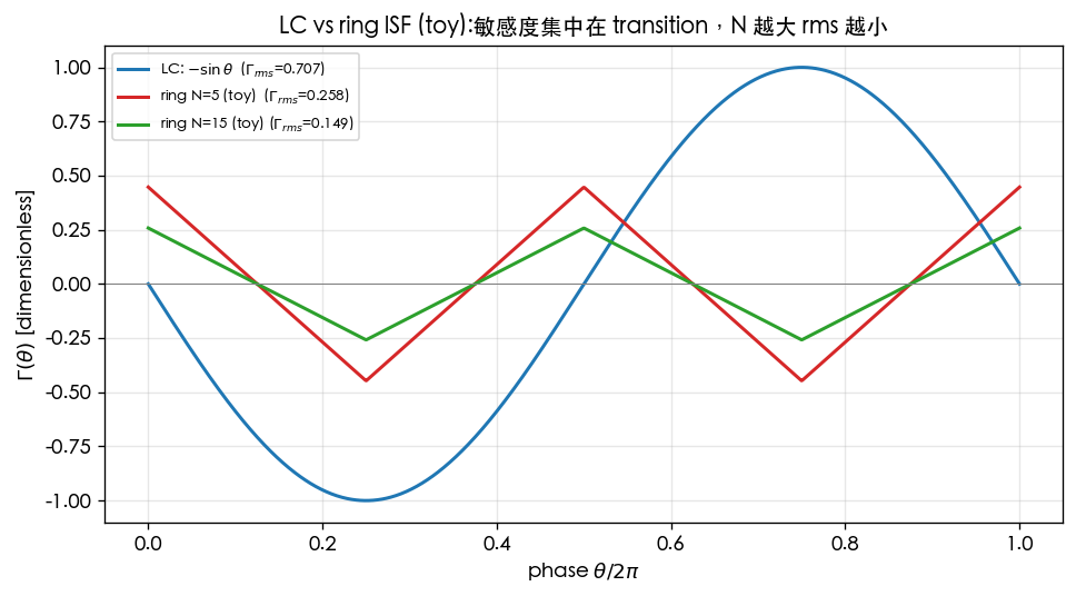
- Conclusion: a ring stage's ISF is concentrated in the narrow phase window of the transition, near zero on the rails. Idealize it as a triangular toy shape — peak at the transition, width roughly equal to the fraction of the period the transition occupies.
This agrees with the triangular toy in lc_vs_ring (gamma_triangular(theta, n_stages), see simulations/common/isf_utils.py):
Comparison figure (ideal LC's vs. ring's triangle):
Why the transition is both the most sensitive and the noisiest instant
Turning observation (b) around: a ring's device carries its largest current during transition (it must rapidly charge/discharge the node capacitance), so the noise modulating function 's peak also lands at the transition. And the ISF 's peak also lands at the transition (just derived above). The two peaks overlap → is barely reduced by windowing ([P1] §IV.D: the ring's and are "almost identical") → cyclostationary effects cannot rescue the ring.
This is one of two main reasons ring phase noise is worse ([P1] states this explicitly): (1) the noise peak overlaps the ISF peak, so cyclostationary effects cannot move noise into an insensitive window; (2) a ring dissipates all its stored energy every cycle (no high- tank to store energy). Compare with Colpitts: its pulse aligns with a small-ISF region — the two peaks are offset — which is why Colpitts is clean.
Device noise → ISF harmonics → close-in PN: the ring stage's full chain (worked example 3)
Example 3 (a ring stage's and floor, order-of-magnitude by hand): a 5-stage CMOS ring, GHz, pC, each inverter stage's equivalent white noise . Estimate using the triangular toy, then compute in the region (single-stage contribution, order of magnitude).
Chain link 1 (slope → ISF): triangular toy, . From the [P2] Eq.(16) scaling (see convention §3), ; for the triangular toy, we take numerically (toy-level order of magnitude; gamma_rms(theta, gamma_triangular(theta, 5)) computes to about — this example rounds to for an integer-order estimate).
Chain link 2 (ISF → close-in PN, [P1] Eq.(21)): at MHz:
- rad/s, .
- .
- .
- Linear value inside parentheses .
- (single-stage order of magnitude).
Chain link 3 (summing over stages): uncorrelated stages each contribute one share, so total power → dB:
Result: single stage dBc/Hz; 5-stage total dBc/Hz @ 1 MHz (order of magnitude).
- Intuition: much worse than (a)'s LC VCO (, single source dBc/Hz) — but note the ring's has already been suppressed by ; the real penalty comes from summing over stages plus the lack of tank energy storage (only the dB multi-stage-summing part is demonstrated here).
- Dimension check: same as [P1] Eq.(21) — the bracket reduces to (per-Hz) ✓.
import numpy as np
import sys, os
sys.path.insert(0, "simulations/common")
from simulations.common.isf_utils import gamma_triangular, gamma_rms
theta = np.linspace(0, 2*np.pi, 4000, endpoint=False)
g_rms = gamma_rms(theta, gamma_triangular(theta, 5))   # computes to ~0.26 (hand calc rounds to integer order 0.30)
qmax, Si = 1e-12, 4e-23
dw = 2*np.pi*1e6
L1 = 10*np.log10((g_rms**2/qmax**2) * (Si/(4*dw**2)))   # single stage
L5 = L1 + 10*np.log10(5)                                 # 5-stage sum
print(round(L1,1), round(L5,1), "dBc/Hz")               # computed ~ -137.7 / -130.7 (hand calc with 0.30 -> -136 / -129)
Design knobs (CMOS ring stage):
- Steep transition (high slew rate) → smaller local , narrower transition window → lowers .
- More stages → decreases (but power, area, and per-stage noise summing all increase — needs trade-off).
- Symmetric rising/falling edges (NMOS/PMOS matched) → suppresses , curbs flicker upconversion (see symmetry).
- A ring has no tank energy storage, and cyclostationary effects offer no help → for the same , close-in performance is inherently worse than LC.
Comparison table across the three topologies
| Dimension | Cross-coupled LC VCO | Colpitts | CMOS ring stage |
|---|---|---|---|
| Tank ISF | (differential, pure ) | (near-sinusoidal) | Triangular, concentrated at transition |
| Main noise sources | (tank), (tail) | Single device (narrow current pulse) | Each inverter stage (large current at transition) |
| Effective ISF | Tank clean; tail rich in | Narrow window (pulse aligned with small-ISF region) | (peak overlaps noise peak) |
| Flicker upconversion () | Tank ; tail large | Depends on symmetry | Depends on rise/fall symmetry |
| fold-back () | Tail has it (needs tail filter) | Weak | Weak |
| Does cyclostationary help? | Tail: no ( are the trouble) | Yes (two peaks offset) | No (two peaks overlap) |
| Close-in order of magnitude (hand-calc worked example) | Tail corner kHz | drops by about 7 dB | 5-stage dBc/Hz @1MHz |
| Key design knob | Symmetry + tail filter @ + large | Align pulse with ISF trough + narrow conduction angle | Steep transition + stage count + symmetric edges |
| Model honesty note | Tank exact / tail illustrative | narrow-window order-of-magnitude estimate | Triangular toy + order of magnitude |
Validity and failure conditions
| Condition | When it holds | What happens when it fails |
|---|---|---|
| Small perturbation, linear phase | , Eq.(21)/(23) hold | Large injection → AM–PM, the ISF itself gets altered |
| Effective ISF uses the correct | Close-in prediction is accurate (including cyclostationary effects) | Using stationary under/overestimates close-in |
| Tail filter is genuinely high-impedance at | fold-back is choked off | Mistuning or insufficient → residual fold-back |
| Waveform symmetry () | Small corner | Asymmetry → large → close-in raised |
| This page's values are illustrative | Demonstrates mechanism and order of magnitude | Precise design needs transistor-level / PSS+PNOISE (Spectre) |
Key takeaways
- The key point for real topologies: each device-noise source sees a different effective ISF ; close-in behavior is set by 's harmonics () and ( fold-back).
- Cross-coupled LC VCO: differential tank ISF (pure , , clean); the tail's effective ISF is rich in (flicker upconversion) and (tail swings at , folded back by switching commutation) → the countermeasure is waveform symmetry + a tail filter tuned to ([P1] §IV.D; Andreani tail-noise, external literature).
- Colpitts: the device current is a narrow pulse; windows down to a narrow phase interval; the pulse aligns with the tank-voltage trough (small-ISF region) → low → clean close-in ([P1] Fig. 13/14, Eq.(27)).
- CMOS ring stage: deriving from transition slope shows it concentrates at the transition (triangular toy); the ISF peak overlaps the noise peak → cyclostationary effects offer no help, and there's no energy storage → close-in is inherently worse.
- The three worked examples each walk the full chain (device noise → ISF harmonics → close-in PN): tail corner kHz, Colpitts narrow-window suppression of by about 7 dB, 5-stage ring dBc/Hz @1MHz (all hand-calculated order of magnitude).
- Sources: [P1] Eq.(21),(23),(24) p.185, Eq.(27) p.186, Fig. 5/13/14; figures
cross_coupled_vco_isf.png(lab_21, illustrative),lc_vs_ring_isf_comparison.png(lab_03).
Further reading
- Effective ISF and cyclostationary effects: effective_isf
- Flicker upconversion to : flicker_noise_upconversion
- How symmetry suppresses : symmetry
- Comprehensive LC vs. ring comparison: lc_vs_ring
- Waveform slope and sensitivity: waveform_slope
- Tank swing and : tank_swing
- Mapping device noise to the ISF: device_noise_mapping
External literature (not among the five source PDFs)
- [E-Andreani] P. Andreani, X. Wang, L. Vandi, and A. Fard, "A Study of Phase Noise in Colpitts and LC-Tank CMOS Oscillators," IEEE J. Solid-State Circuits, vol. 40, no. 5, pp. 1107–1118, May 2005. (The authoritative analysis of tail noise and cross-coupled vs. Colpitts phase noise; the basis for this page's arguments about tail fold-back and the tail filter. Volume/issue/pages verified (DOI 10.1109/JSSC.2005.845991).)
- The classic source for the tail filter @ is also E. Hegazi, H. Sjöland, A. A. Abidi, "A Filtering Technique to Lower LC Oscillator Phase Noise," IEEE JSSC, vol. 36, no. 12, pp. 1921–1930, Dec. 2001. (Not among the five source PDFs; volume/issue/pages verified.)