β: This English translation is in beta — the Traditional-Chinese original is the authoritative version.
Tuning-line and supply-pushing phase noise
Prerequisites (read these first): white_noise_to_phase_noise (white noise → via the integrator), flicker_noise_upconversion ( → ; this page draws the parallel), phase_vs_amplitude_noise (the AM-PM back door). This page assumes you already accept the main thread: "phase has no restoring force → noise integrates through into the skirt."
Everything in the ISF framework so far has been about the device's own noise current injected directly into the tank node. But a real VCO (voltage-controlled oscillator — output frequency set by a control voltage) has two more phase-noise gates that don't rely on the device's internal at all, but on jitter of an external voltage node:
- tuning line: you use a voltage to tune the varactor (a varactor diode — bias changes its capacitance) and set to the desired channel. Any noise voltage on this line directly FM-modulates (frequency-modulates) the carrier.
- supply (): supply voltage variation changes the effective via the device operating point, parasitic capacitance, and similar paths — this is called supply pushing (supply voltage pushes the oscillation frequency around).
This page answers: how do these two external voltage gates turn low-frequency noise voltage into close-in phase noise? Why does the mechanism look identical to device flicker's ? And how do design choices close these two gates down?
Physical intuition (the punchline first): think of the VCO as a "voltage → frequency" converter with sensitivity (Hz/V). A noise voltage on the control node jitters the instantaneous frequency by . Frequency is the derivative of phase, so phase is the integral of frequency — this integrator is the exact same machine that turns (voltage noise) into the skirt in the ISF white-noise result: literally the same integrator. Hence: white noise on the tune line → ; noise on the tune line → . The larger , the wider this gate opens; shrinking it (coarse tuning via switched-cap, fine tuning via varactor) and cleaning up (LDO, common-mode rejection) is the core of every design knob on this page.
The concrete circuit/topology/instrumentation details on this page — the varactor – model, LDO/cross-coupled VCO topology specifics, measurement methods — belong to standard RF IC design literature (Razavi, Leeson, vendor datasheets); not among the five source PDFs on this site, and this page explicitly flags them "(external literature, not among the five source PDFs)." But the main thread — "voltage noise → FM → phase skirt" — follows strictly from [P1]'s existing phase-integration concept alone, which is what we do below.
Step 1: define and supply pushing
A VCO is by definition "output frequency varies with control voltage." Treat oscillation frequency as a function of control voltage and supply , and do a first-order Taylor expansion about the operating point:
The two slopes are this page's two protagonists:
- (VCO gain, also called tuning sensitivity): how far frequency moves per 1 V of control voltage. It sets the tuning range (the frequency span it can sweep) and also the gain applied to tune-line noise — the core tension on this page: must be large enough to cover the band, yet small enough not to amplify noise.
- (supply pushing coefficient): how far frequency moves per 1 V of supply variation. Ideally the VCO is supply-immune (); in practice the supply alters via device bias point, parasitic capacitance, and effective swing, so . (Vendors often quote a pushing figure in or — external literature, not among the five source PDFs.)
- Dimension check: ✓. Both have the same dimension and are exactly parallel mathematically — every derivation below applies verbatim to tune line and supply; just swap for .
- Physical meaning: these two coefficients connect the "external voltage world" to the "frequency world." They are designer-controllable — unlike the device's (fixed by process/physics), and are outcomes of topology and bias choices.
Division of labor with ISF : ISF handles "a current impulse injected at what phase of the tank node → how much phase shift"; handles "a quasi-static (slow relative to the carrier) control/supply voltage → how much frequency shift." Tune/supply noise is slow (offset ), so it need not go through ISF's per-impulse phase projection — it takes the more direct FM route: "voltage → frequency → integrate into phase." Both routes ultimately converge on the same integrator (see end of Step 2) — exactly the parallel this page draws.
Step 2: how voltage noise FM-modulates the carrier →
Let the tune node carry a low-frequency noise voltage (offset frequency , so it's nearly constant over one carrier cycle — the quasi-static assumption holds). Derive step by step.
Step 2.1: voltage noise → instantaneous frequency deviation. By the definition of , the instantaneous oscillation frequency jitters with :
- Dimension check: ✓ (the angular-frequency version, multiplied by , gives rad/s ✓).
- This is FM (frequency modulation): the control voltage directly modulates the carrier's instantaneous frequency.
Step 2.2: frequency is the derivative of phase → phase is the integral of frequency. The excess phase is by definition "the time integral of the instantaneous frequency's deviation from nominal":
- This integrator is the key point: it is the same integrator [P1] Eq.(11)/(13) uses to integrate into — only here the integrand is not "" but "." Integration = multiply by in the frequency domain (basic signals-and-systems), so power multiplies by — the next step relies on exactly this.
- Physical meaning: phase has no restoring force (phase_vs_amplitude_noise, Step 1), so a "slowly drifting frequency" gets accumulated indefinitely into an ever-growing phase offset — the closer the offset is to the carrier, the larger the integrator gain , and the higher the skirt.
Step 2.3: take the PSD (the integrator is in the power domain). For an LTI system , the effect on input PSD is . Here , so :
The right-hand form uses to cancel the 's (numerator , denominator ), so computing in Hz is cleaner: .
- Dimension check: , and phase is dimensionless (rad), so is ✓. (Strictly, the "dimensionless phase" carried by is implicit; FM phase is inherently dimensionless.)
- Side by side with the ISF white-noise result — white_noise_to_phase_noise's signature formula and this page's both have in the denominator. The device-noise version's "conversion gain" is (A → rad); the tune-line version's is (V → rad/s, then integrated). Same integrator, different entry point — this is the structural isomorphism this page wants you to remember.
Step 2.4: apply SSB phase noise (small-angle approximation). Using the site-wide convention (spec Section 3, Eq. 16):
The supply version is completely parallel: substitute , (supply-voltage noise PSD). The two gates' contributions are independent sources, so powers add: .
Step 3: white tune-line noise → ; tune-line noise → (paralleling device )
Step 2's carries the tune line's spectral shape through unchanged, then multiplies by . Two cases:
Case A — tune line is white noise ( constant): e.g. series-resistor thermal noise, wideband buffer noise. Then
This has exactly the same slope, exactly the same mechanism as device white noise's via ISF (both: white entry → integrator).
Case B — tune line is noise (): e.g. low-frequency flicker from a charge pump / bandgap / LDO reference, or in the varactor bias circuit. Then
This is precisely the "external-voltage version" of the device flicker mechanism. Put the two paths side by side:
| Mechanism | Entry (low-frequency source) | Upconversion "gate" | formula skeleton |
|---|---|---|---|
| device flicker ([P1] Eq.(23)) | device current | ISF's DC term | |
| tune/supply (this page) | control-voltage noise | VCO gain (or ) |
- Where the parallel lies: the device version's "gate" is ISF's DC Fourier coefficient (flicker_noise_upconversion, Step 2: " is flicker's only gate to the carrier"); the tune-line version's "gate" is . The role plays in the external-voltage world is exactly the role plays in the device-current world — both are conversion gains that "connect a low-frequency source to the integrator," and both enter squared ( vs ).
- The difference (stated honestly): the device version's can be pushed close to 0 via waveform symmetry (this rescues flicker); the tune-line version's cannot be zeroed (zero means the frequency can't be tuned at all) — it can only be shrunk (split tuning) or have its entry cleaned up (LDO). So this gate is "permanently half-open," which makes it a design problem that demands direct attention.
- Slope mnemonic: each extra factor in the denominator adds dB/dec. White entry + integrator = (); entry (one extra ) + integrator = (). Identical bookkeeping to the device side.
Step 4: varactor nonlinearity → AM-PM
So far has been treated as constant. But the varactor is inherently a nonlinear capacitor — this opens a second, more subtle gate: AM-PM conversion (amplitude modulation converted to phase modulation), the back door discussed in phase_vs_amplitude_noise, Step 4.
Mechanism chain (each link uses an existing concept):
- Frequency is set by the tank's total capacitance: LC oscillation , where includes the varactor's .
- The varactor sees "bias + oscillation swing": the node voltage is ; a sinusoidal swing of amplitude sweeps across the curve every cycle.
- Nonlinearity → effective capacitance varies with swing: because is curved, the average effective capacitance over one cycle changes with amplitude (Taylor-expand about the bias point; the second-order term is proportional to and nonzero). Hence becomes a function of amplitude, .
- This is exactly : amplitude noise (which would normally be squashed by the limit cycle's restoring force) leaks into frequency/phase noise via , then gets permanently accumulated by Step 2's integrator into a close-in skirt.
- Physical meaning: amplitude noise that was originally "suppressed" (phase_vs_amplitude_noise argues amplitude has a restoring force) escapes through this varactor-curvature back door, coming back to life as long-lived phase noise — in particular, it upconverts the device's amplitude fluctuations into the close-in region, worsening .
- Key design corollary: AM-PM is proportional to (curve curvature), not (slope, which is ). So biasing at the inflection/flat point of can drive , greatly reducing AM-PM — a different knob from "shrink " (one controls curvature, the other controls slope).
- Units/dimension: is ; multiplied by amplitude noise (V) gives rad/s, then integrates into phase ✓.
- Detailed amplitude-modulation and large-signal analysis is the main subject of [P4] (advanced); the exact closed form of varactor belongs to device literature (external literature, not among the five source PDFs). This page only connects the chain to the existing AM-PM concept.
Step 5: design knobs (closing both gates)
Translate the physics above directly into actionable knobs. Each knob states which quantity it acts on.
- Split tuning — shrinks . The single most important technique (external literature, not among the five source PDFs). Split tuning into two layers:
- coarse: switched-capacitor bank (an array of switched capacitors, switched in/out by a digital code). It selects the band with a digital code, providing most of the tuning range, but is immune to continuous voltage noise (the code doesn't jitter, so the capacitance doesn't jitter).
- fine: varactor, responsible only for continuous fine-tuning within a small sub-band.
- Effect: total tuning range = coarse (digital, noise-free) ⊕ fine (small range), and the fine varactor's drops sharply because it only spans a small sub-band. By Step 2's , halving cuts the tune-line phase-noise contribution by 6 dB. This is the standard way to untangle the "range vs. noise" tension.
- Bias at the flat point of — suppresses AM-PM (controls ). Choose the varactor operating point so (small curvature), driving and closing the AM-PM back door. Note this is a different knob from shrinking : the flat point suppresses second-order curvature, not first-order slope.
- Supply regulation / LDO — suppresses the entry (external literature, not among the five source PDFs). To combat supply pushing: place an LDO (low-dropout regulator) ahead of the VCO to filter a dirty supply into a clean local supply, reducing (the supply-noise PSD reaching the VCO) by tens of dB. By the supply-side formula , reducing reduces phase noise proportionally. You can also reduce itself (topology-level: symmetric bias, less supply-to-swing modulation).
- Common-mode rejection — makes a differential VCO immune to common-mode supply/substrate noise. On a differential tank, supply/substrate noise mostly appears as a common-mode disturbance; good differential symmetry keeps common-mode disturbances from converting to differential-mode frequency shifts (ideally ). This shares its origin with flicker_noise_upconversion Step 6's differential concept, but here it combats external common-mode voltage rather than device .
- Clean routing — suppresses the entry. Loop-filter resistor thermal noise, charge-pump , and bandgap reference noise all feed into ; these are the physical origin of the "in-band" terms in pll_noise_budget. Within a PLL, the loop bandwidth also determines how much this tune-line noise gets high-pass/low-pass filtered.
Design rule of thumb (in one line): the phase noise from these two gates = (conversion gain ) × (entry voltage noise ) × ( integrator). Each of the three factors has its own knob: suppress with split tuning / symmetric topology, suppress with LDO / clean reference / low-noise loop filter, and suppress the curvature-driven AM-PM with a flat bias point.
Worked example (with units + dimension check)
Example G (tune-line white noise → ): MHz/V, tune-line voltage noise nV (i.e. nV) at MHz offset, GHz. Find .
Step 1 (square into a PSD):
Step 2 (voltage noise → frequency-deviation density, for intuition): the rms density of frequency deviation . In other words, at 1 MHz offset this tune line jitters the frequency by "5 Hz per ."
Step 3 (apply Step 2's , in Hz form):
Step 4 (SSB): , take :
- Result: dBc/Hz — this single tune-line white-noise source alone contributes dBc/Hz. Compared with the canonical "single device white-noise source" Example B ( dBc/Hz, white_noise_to_phase_noise), the tune line is nearly 40 dB higher at the same offset — showing that one poorly handled tune line can easily dominate a whole VCO's region, which is exactly why split tuning / a clean matter so much.
- Dimension check: → is ✓.
- Where did GHz go? (honesty note): this formula's does not explicitly contain — only tells you which carrier this skirt sits on; the skirt's height is set by , independent of . genuinely enters when converting to timing jitter (, see psd_phase_noise_jitter), or when expressing 's relative sensitivity in . GHz is given so you know this is a 5 GHz VCO, but don't force it into the formula.
import math
K_vco = 50e6          # Hz/V
S_v   = (100e-9)**2   # V^2/Hz  (100 nV/sqrt(Hz))
df    = 1e6           # Hz offset
S_phi = K_vco**2 * S_v / df**2          # rad^2/Hz
L     = 10*math.log10(0.5*S_phi)        # SSB, L = (1/2) S_phi
print(S_phi, L)        # -> 2.5e-11 rad^2/Hz, -109.03 dBc/Hz
Example H (supply pushing → , parallel verification): MHz/V, supply noise () at MHz. Find the supply contribution to .
- Intuition: even though is 25x smaller than , a "mere" dirty supply still contributes dBc/Hz. Add an LDO that cuts by 20 dB (a 10x reduction in voltage noise), and this contribution drops 20 dB to dBc/Hz — the direct payoff of an LDO against supply pushing.
- Dimension check: same as Example G, → ✓.
# supply pushing parallel version: same formula, K_vco->K_push, S_v->S_vdd
K_push, S_vdd, df = 2e6, (1e-6)**2, 1e6
S_phi = K_push**2 * S_vdd / df**2
print(10*math.log10(0.5*S_phi))   # -> -117.0 dBc/Hz
K_push from first principles (Level-1 ring measurement, lab_38)
Example H's MHz/V was a given representative value (a well-cared-for LC-VCO grade number). This section gives nothing: take the MOS Level-1 (Shichman-Hodges square-law) 3-stage ring from lab_32 and measure directly by its definition — first a static sweep for the slope of , then a small superimposed ripple to verify Step 2's FM-integrator prediction. Honesty statement: this is device-equation level (Level-1 square law, ), NOT SPICE/BSIM/PDK; the numbers belong to this toy ring, but the physics and the order-of-magnitude lesson are general. Full script: simulations/lab_38_supply_pushing_ring.py (the node equation reuses lab_32 bit-exactly, only promoting to an argument; cross-check difference V/s).
Static measurement: sweep →
Sweep from 0.9 V to 1.1 V (25 mV grid); at each point let the ring reach steady oscillation and measure the period by threshold crossings:
| [V] | 0.900 | 0.950 | 1.000 | 1.050 | 1.100 |
|---|---|---|---|---|---|
| [GHz] | 0.9394 | 1.0803 | 1.2252 | 1.3738 | 1.5255 |
GHz exactly reproduces lab_32 (same ring, same integrator). Central difference at 1.0 V:
(The 9-point quadratic-fit derivative gives 2.932 GHz/V, 0.1% apart — the slope extraction is self-consistent.) Dimension check: Hz ÷ V = Hz/V ✓.
Why so large? A hand sanity check (step by step): the ring's frequency is (the concept of [P2] Eq.(15); this 2 is the circuit fact "two edges per period," not a bookkeeping convention), and each stage delay is , where the swing and the drive current follows the square law . Hence
(The 2 in the numerator is the square-law exponent — a physical origin, not a convention.) Plug in V, V: , times GHz gives 2.859 GHz/V — 2.6% from the measured 2.936 GHz/V; both magnitude and physics agree. Dimension check: ✓.
The normalized pushing is /V ppm/V. For contrast: an LC VCO's is set by the tank's and the supply only perturbs it through parasitics and bias (typical pushing figures sit in the ppm/V to thousands-of-ppm/V range — external literature, not among the five source PDFs); a ring's is device current divided by capacitance — the supply sits directly inside the formula. "A ring's supply pushing is inherently orders of magnitude larger than an LC's" is not folklore; it is a direct consequence of .
Dynamic verification: 10 mV ripple → narrowband FM sidebands
Superimpose a sinusoidal ripple mV at MHz on . By Step 2's integrator, step by step:
The peak phase deviation (FM modulation index) is . Dimension check: dimensionless (rad) ✓ — exactly the FM fundamental "frequency deviation ÷ modulation frequency = phase." Plug in the measured value:
The simulation puts the ripple physically into the node equation, extracts from threshold-crossing times, and fits a sinusoid: rad, ratio 1.002 (modulation phase , theory : ✓). The spectrum shows sidebands at : measured dBc, against the narrowband-FM prediction dBc (exact Bessel value dBc). Convention flag: this is FM math () — it is not the same 2 as the SSB bookkeeping in , nor the 4 in the denominator of [P1] Eq.(21). The 0.52 dB upper/lower sideband asymmetry is concurrent AM (the swing itself tracks , ) — a supply-side miniature of Step 4's AM-PM issue; even the second-order sidebands at ( dBc) match 's dBc.
This deterministic single-tone experiment verifies precisely Step 2's integrator: a random is nothing but a superposition of countless such tones (in PSD language), so " checks out" is equivalent to " checks out."
# lab_38 key numbers (reproduce with: PYTHONPATH=. python simulations/lab_38_supply_pushing_ring.py)
K_push = (1.2991e9 - 1.1523e9) / 0.05
print(f"{K_push:.3e}")   # -> 2.936e9 Hz/V (central difference @ 1.0 V)
beta   = K_push * 10e-3 / 100e6
print(round(beta, 4))         # -> 0.2936 rad (measured 0.2942, ratio 1.002)
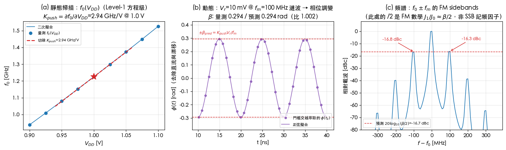
How to read the figure: (a) is nearly a straight line (slightly curved); the red tangent's slope is ; (b) extracted from threshold crossings (purple dots) with the sinusoidal fit; the red dashed lines are pure theory, not fitted; (c) the spectrum normalized to the carrier at 0 dB — the MHz sidebands land on the predicted level, and the small peaks at MHz are second-order FM sidebands. Parameters: fF/node, , static sweep fs, dynamic fs, 150 ns record; runtime about 28 s.
Example I (end-to-end: measured × this page's formula): take Example H's same supply noise, () at MHz, but substitute this ring's measured GHz/V:
(The here is the SSB small-angle convention , spec Section 3, Eq. 16.) Dimension check: → rad²/Hz ✓. This is 63.3 dB worse than Example H's dBc/Hz — exactly , entirely from the square of . That is the quantitative version of "an unregulated ring on a dirty supply is a disaster"; conversely, the is also good news: every 20 dB an LDO shaves off the voltage noise removes 20 dB of this phase-noise contribution.
Interface with the ISF: the supply sees the "coherent sum of per-stage sensitivities"
In ISF language there is one key difference between device noise and supply noise:
- device noise (each stage's own ): the stages' noise sources are mutually independent, so per-stage contributions add in power — this is [P2]'s bookkeeping for the ring analysis (one share per stage).
- supply (the rail): the supply is a port shared by all stages. One low-frequency (quasi-static) supply disturbance changes every stage's delay simultaneously and in the same direction — whichever stage is switching gets sped up or slowed down by the same , and within one period the delay changes of all edges accumulate with the same sign into . So the supply's effective sensitivity is the coherent (amplitude) sum of the per-stage sensitivities, and the average (DC) component of that sum is exactly : for a slow disturbance, "some stage is being pushed at every instant," and the summed sensitivity never changes sign.
- Corollary 1: stacking independent sources scales as (power addition); a coherent source scales as (amplitude addition) — supply noise is not merely "one more noise source": it bypasses the statistical discount of independent sources.
- Corollary 2: the DC term of the supply's effective sensitivity is inherently large (its role is that of in device-flicker upconversion), so the supply's noise upconverts to as in Step 3; but while the device version can push near 0 via waveform symmetry (lab_32's symmetric ring measured ), the supply version has no such card to play — "every stage's delay tracks " is not something symmetry can cancel. The remaining cards are suppressing the entry (LDO) and suppressing itself (differential/regulated topologies, stage designs whose delay is first-order insensitive to — external literature, not among the five source PDFs).
Limitations (honestly): Level-1 square law, , a single lumped , single point (no -scaling verified); a real PDK ring's number will differ due to velocity saturation and short-channel effects (though it remains far larger than an LC's — external-literature experience), while this section's method (definition-based measurement + FM verification) and structural conclusions (coherent summing, the lever) stand.
Validity and failure conditions
| Condition | When it holds | What breaks when it doesn't |
|---|---|---|
| Control/supply noise is slow (, quasi-static) | constant, FM model holds | At high frequency (near ) must fall back to ISF/HTM's per-harmonic treatment |
| is approximately linear at the operating point | A single slope suffices | Strong varactor nonlinearity → varies with and generates AM-PM (Step 4) |
| Small perturbation, linear phase | holds | Large voltage swing → higher-order FM sidebands, spectral distortion |
| AM-PM negligible () | "FM only" approximation is good | Strong curvature → amplitude noise revives as phase noise; needs the [P4] APF framework |
| Sources independent | Powers add directly, | Correlated sources (shared reference) need cross terms; common-mode rejection can help |
Corresponding papers/formulas
- The phase integrator and its structural link to device white noise's and flicker's : [P1] Eq.(11)/(13), p.182–183 (phase is the integral of noise), Eq.(21) p.185 (), Eq.(23) p.185 (, gate). This page draws the analogy " gate" ↔ " gate."
- AM-PM / amplitude modulation's full framework: [P4] (APF, amplitude decay, advanced; see phase_vs_amplitude_noise).
- definitions, split tuning, switched-cap bank, LDO, varactor , common-mode rejection, pushing figure and other circuit/topology/instrumentation specifics: standard RF IC design literature (external literature, not among the five source PDFs) — Razavi's RF Microelectronics, the Leeson model, vendor datasheets.
- : spec Section 3, Eq. 16 (small-angle PM).
- first-principles measurement (lab_38): the ring frequency concept comes from [P2] Eq.(15), p.794; the device equations and the ring itself reuse lab_32 (Level-1 equation level, NOT SPICE/BSIM/PDK); narrowband FM's is standard communications-textbook material (external literature, not among the five source PDFs).
Key takeaways
- , (both Hz/V): the conversion gains connecting the external-voltage world to the frequency world.
- Noise voltage on the tune/supply node FM-modulates the carrier: → phase is the integral of frequency → (using the same integrator as ISF white noise).
- White tune-line noise → ; tune-line noise → . 's role in the external-voltage world ISF's 's role in the device-current world (both enter squared), but cannot be zeroed, only shrunk.
- Varactor nonlinearity → AM-PM: , reviving suppressed amplitude noise as phase noise; a flat bias point (small ) suppresses it (a different knob from shrinking ).
- Design knobs: split tuning (coarse switched-cap + fine varactor, shrinks ), flat bias point (suppresses AM-PM), LDO / clean reference (suppresses the entry), common-mode rejection (combats supply/substrate common mode).
- Numbers: MHz/V, nV @ 1 MHz → dBc/Hz (a single tune line alone can dominate the region); does not explicitly contain .
- lab_38 first-principles measurement: the Level-1 3-stage ring measures GHz/V ( ppm/V; the hand square-law model is 2.6% away); the 10 mV @ 100 MHz ripple FM verification gives ; with the same supply, dBc/Hz — 63.3 dB worse than Example H. A ring's supply sees the "coherent sum of per-stage sensitivities," has no symmetry-zeroing card to play, and must rely on LDO/regulated topologies.
Further reading
- The common origin of the integrator and white-noise : white_noise_to_phase_noise
- The → mechanism this page parallels: flicker_noise_upconversion
- The AM-PM back door and why amplitude noise is normally suppressed: phase_vs_amplitude_noise
- How tune-line noise is high-pass/low-pass filtered in the loop, and optimal loop BW: pll_noise_budget
- The swing/ lever (another independent knob): tank_swing
- Which knobs change and which change : device_noise_mapping
- The Level-1 ring used by lab_38, and its ISF extraction: lab_32_mos_level1_ring
- The high-frequency entrance for supply/substrate noise — correlated noise only enters from near DC and ([P2] Eqs.(37)–(38) selection rule; this page's is precisely the DC tooth of that comb): lab_34_correlated_supply