Lab 09 — 設計取捨綜合 scaling
前面八個 lab 把每個機制各別跑通了。這個綜合 lab 不引入新模擬,而是把 [P1] Eq.(21) 這條招牌式當成設計旋鈕地圖:固定其他條件,分別掃 、、 ring 級數 ,看 phase noise 與 rms jitter 怎麼動。 全程用 canonical 數值(規範第 8 節)做口算,建立「動哪個旋鈕、賺幾 dB」的反射。
物理直覺(先講結論): phase noise 。 想降相位雜訊只有兩條大路:把訊號電荷 做大(多存能量,雜訊相對變小), 或把 ISF 做小(讓波形對雜訊不敏感)。 兩者都是 的關係: 加倍 → 相位雜訊 dB; 減半 → 也是 dB。ring 振盪器的 同時動兩件事,要小心淨效果。
1. 教學目標
- 把 [P1] Eq.(21) 讀成 scaling law,建立 、、 的設計直覺。
- 用 canonical 數值算出「動一個旋鈕賺幾 dB / 幾 fs」。
- 看懂 ring 振盪器 的雙面性(,但功率/面積也漲)。
- 把 scaling 結論連到各 design insight 頁。
2. 數學模型
起點是 [P1] Eq.(21), p.185:
把對數展開成「相加的旋鈕」(固定 、):
- 讀法:每個旋鈕都是 (電壓/電荷類)或 (功率類)。 與 都進 ,所以「加倍/減半 = dB」。
jitter 與 phase noise 同源:對 skirt, (規範公式 19),而 ,所以
- dB 與 jitter 的橋: 降 dB(功率 )→ 減半()。
ring 振盪器:[P2] 給出兩條 scaling——級數越多,每級 ISF 越尖但 rms 越小([P2] Eq.(16), p.794):
- 單看 phase noise, 從 5 → 15(): 乘 , 變化 dB。但級數多 → 功率、面積、 分配都變, 且 下降(除非縮 ),所以這只是「孤立看 」的 toy scaling,非淨設計結論。
3. Block diagram
4. Python 核心 code
本 lab 不產生新圖,scaling 直接用 [P1] Eq.(21) 口算。下面這段(沿用
simulations/lab_08_jitter_integration.py 的習慣)示範如何把旋鈕變化換成 dB 與 fs,
讓你能自己掃參數:
import math

def L_dbc(Grms, qmax, Si, df):
    """Hajimiri-Lee Eq.(21): 1/f^2 SSB phase noise [dBc/Hz]."""
    dw = 2 * math.pi * df
    return 10 * math.log10((Grms**2 / qmax**2) * (Si / (4 * dw**2)))

# canonical baseline (規範例 B)
f0, df, Si = 5e9, 1e6, 1e-24
base = L_dbc(Grms=0.5, qmax=1e-12, Si=Si, df=df)   # -148.0 dBc/Hz

print("baseline           :", round(base, 1), "dBc/Hz")
print("q_max x2           :", round(L_dbc(0.5, 2e-12, Si, df) - base, 1), "dB")  # -6.0
print("Gamma_rms /2       :", round(L_dbc(0.25, 1e-12, Si, df) - base, 1), "dB") # -6.0
# ring N: Gamma_rms ~ N^-1.5 ([P2] Eq.(16), p.794, re-verified v7: sqrt covers only the constant); show isolated scaling
for N in (5, 15, 45):
    rel = (N / 5.0) ** -1.5
    print(f"N={N:2d} Gamma_rms rel={rel:.3f}  dL={20*math.log10(rel):+.1f} dB")

# jitter scales as Gamma_rms / q_max  ->  -6 dB phase noise = sigma_t / 2
L_dbc與 lab_08 的integrate_rms_jitter不同:lab_08 從 積分出 jitter; 這裡反向用 Eq.(21) 產生 ,再用 scaling 推 jitter。兩頁互為正反操作。
5. 完整 script path
本 lab 為綜合分析,無專屬 script。引用的計算來自:
simulations/lab_06_white_noise_phase_noise.py( scaling 的模擬證據)、
simulations/lab_03_ring_toy_model.py(LC vs ring ISF 與 scaling)、
simulations/lab_08_jitter_integration.py()。
上面的口算片段可存成獨立小腳本自行掃參數。
6. 參數表
| 參數 | 符號 | canonical 值 | 角色 |
|---|---|---|---|
| 載波頻率 | GHz | 固定 | |
| offset | MHz | 固定(評估點) | |
| 電流雜訊 PSD | A²/Hz | 固定(單一白噪源) | |
| 最大電荷擺幅 | pC(基準) | 旋鈕 1,掃 pC | |
| ISF rms | (基準) | 旋鈕 2,掃 | |
| ring 級數 | (基準) | 旋鈕 3,掃 | |
| 基準相位雜訊 | dBc/Hz | 由 Eq.(21) 得(=規範例 B) |
7. 單位表
| 量 | 符號 | 單位 |
|---|---|---|
| 最大電荷擺幅 | C | |
| ISF rms | 無因次 | |
| ring 級數 | 無因次 | |
| 相位雜訊 | dBc/Hz | |
| rms jitter | s | |
| 電流雜訊 PSD | A²/Hz |
8. scaling 表(口算,toy scaling)
以 canonical 基準 dBc/Hz( pC、、 、5 GHz @ 1 MHz)為 dB 參考。。
| 旋鈕變化 | 變化 | 變化 | 物理理由 |
|---|---|---|---|
| ( pC) | dB | ;訊號電荷大、雜訊相對小 | |
| ( pC) | dB | 同上反向 | |
| () | dB | ;波形對雜訊不敏感 | |
| ring () | dB | (孤立看,[P2] Eq.(16), p.794,v7 已重核) | |
| ring () | dB | 同上;但功率/面積/ 也一起變 |
口算示範: 從 1 pC 加倍到 2 pC, 改變 dB → dBc/Hz;jitter 隨 減半。 把 lab_08 的 fs(那是 dBc/Hz 的情境)做同樣 dB 操作,會降到 fs。
9. 如何解讀圖(重用既有圖)
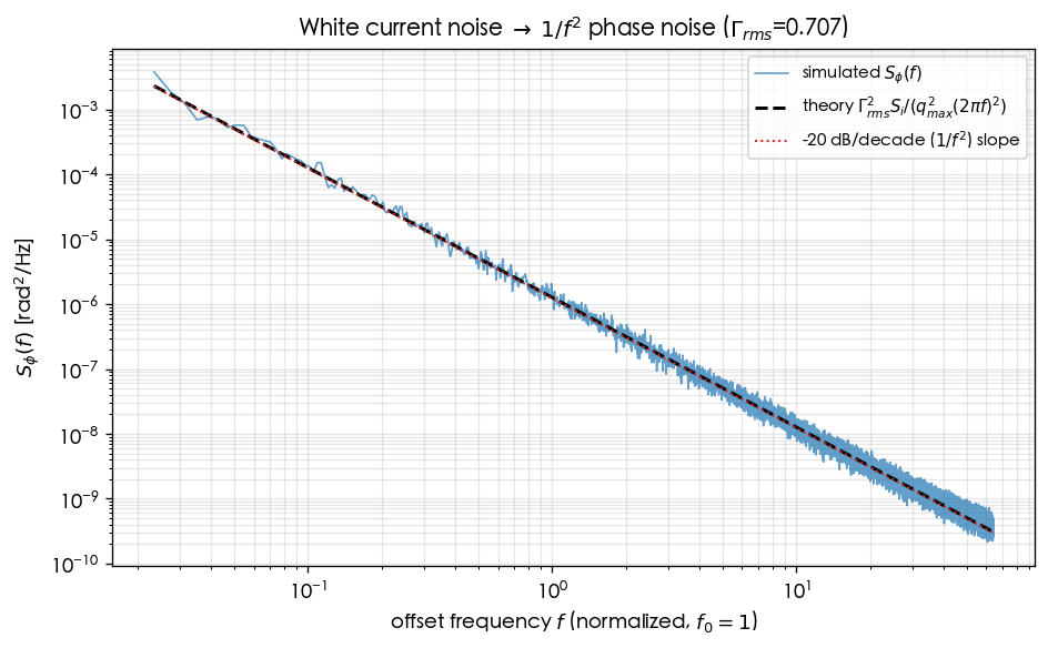
圖一: scaling 的模擬證據。 lab_06 的白噪 PSD 圖,把 ISF 換成不同 (或改 )時,整條 線只是上下平移,斜率不變——這就是 scaling 表 「動旋鈕 = 平移 dB」的視覺版。
圖二:LC vs ring 的 ISF 形狀與 。 lab_03 的對比圖:ring 的 ISF 敏感度集中在 transition, 越大每級 ISF 越尖、但 rms 越小()。這解釋了 scaling 表 旋鈕 3 的來源,也提醒這是孤立 scaling。
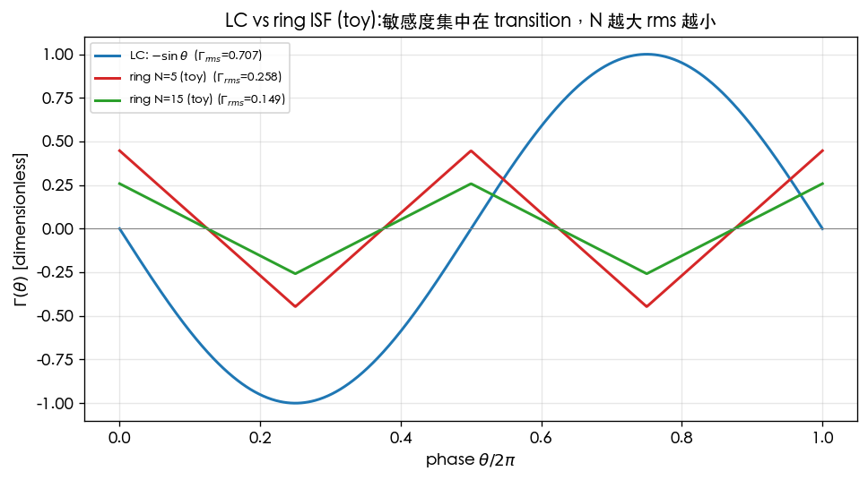
- 怎麼用兩張圖:圖一告訴你「/ 旋鈕 = 垂直平移」; 圖二告訴你「ring 的 怎麼隨 變」。合起來就是設計地圖。
10. 對應 paper 公式/figure
- 主 scaling:[P1] Eq.(21), p.185,。
- Parseval / :[P1] Eq.(20), p.185。
- ring scaling:[P2] Eq.(16), p.794(v7 已重核:根號只蓋常數,; 正文 4/N^1.5@η=0.75 與 App.B Eq.(55) 三重驗證。v3 曾誤讀為 N^-0.75)。
- ring 頻率:[P2] Eq.(15), p.794,。
- ring 白噪 FOM:[P2] Eq.(23), p.796,( 為級延遲比例常數 [P2] Eq.(14),; 僅透過 進入)。
- 概念圖:重用
white_noise_phase_noise_psd.png(lab_06)與lc_vs_ring_isf_comparison.png(lab_03)。
11. 限制與 approximation
- toy scaling,非 transistor-level:scaling 假設「只動一個旋鈕、其他完全不變」。 真實電路裡 、、、功率、面積、 彼此耦合,不能孤立調。
- ring scaling([P2] Eq.(16), p.794,v7 已重核:根號只蓋常數,; 正文 4/N^1.5@η=0.75 與 App.B Eq.(55) 三重驗證。v3 曾誤讀為 N^-0.75): ();級數變多也改 、功率與面積,淨 phase noise/jitter 要看完整 FOM,不能只看 。
- 單一白噪源:忽略多源、cyclostationary()、flicker 上轉 (,見 lab_07)。close-in 區此表不適用。
- factor-of-2:用 Eq.(21) 的分母 ;與時域版差 SSB 記帳 2 倍, 不影響任何 scaling 結論(所有 dB 變化都是相對量)。
- jitter scaling: 假設固定積分範圍與 形狀; 若 close-in 主導,jitter 由 與積分下限決定,需另算。
重點回顧
- phase noise ;jitter 。
- 加倍或 減半 → phase noise dB、jitter 減半()。
- ring 孤立看 ( dB),但 /功率/面積同時變,是 toy scaling。
- 基準數字: pC、、5 GHz @ 1 MHz、 → dBc/Hz。
延伸閱讀
- 設計:power_and_qmax
- 對稱性砍 :symmetry_and_1overf
- SerDes 時脈:serdes_clocking_connection
- 用在設計/理論:把 、、 的 scaling 落到拓樸抉擇 → lc_vs_ring
- 上游模擬:lab_06_white_noise_phase_noise、 lab_08_jitter_integration