β: This English translation is in beta — the Traditional-Chinese original is the authoritative version.
Lab 09 — Design trade-off scaling synthesis
Breadcrumb: Simulation labs › Noise & jitter › This page (design trade-offs intro). Upstream: lab_06, lab_08; advanced version: lab_17.
The first eight labs exercised each mechanism one at a time. This synthesis lab introduces no new simulation; instead it treats [P1] Eq.(21) — the signature equation — as a map of design knobs: holding everything else fixed, separately sweep , , and the ring stage count , and watch how the phase noise and the rms jitter move. Throughout we use the canonical numbers (spec Section 8) for back-of-envelope arithmetic, building the reflex of "turn this knob, gain that many dB".
Physical intuition (conclusion first): phase noise . There are only two broad roads to lower phase noise: make the signal charge larger (store more energy, so the noise is relatively smaller), or make the ISF smaller (make the waveform insensitive to noise). Both are relationships: doubling → phase noise dB; halving → also dB. A ring oscillator's moves two things at once — watch the net effect carefully.
1. Learning objectives
- Read [P1] Eq.(21) as a scaling law and build design intuition for , , and .
- Use the canonical numbers to compute "how many dB / how many fs one knob buys".
- Understand the two-sided nature of the ring oscillator's (, but power/area grow too).
- Connect the scaling conclusions to the design-insight pages.
2. Mathematical model
The starting point is [P1] Eq.(21), p.185:
Expand the logarithm into "additive knobs" (fixing and ):
- How to read it: every knob enters as (voltage/charge-like) or (power-like). Both and enter through , so "double/halve = dB".
Jitter and phase noise share the same origin: for the skirt, (spec formula 19), and , so
- The bridge from dB to jitter: down dB (power ) → halves (the ).
Ring oscillator: [P2] gives two scalings — more stages make each stage's ISF sharper but its rms smaller ([P2] Eq.(16), p.794):
- Looking at phase noise alone, from 5 → 15 (): is multiplied by , a change of dB. But more stages → power, area, and the allocation all change, and drops (unless shrinks), so this is a toy scaling that "looks at in isolation", not a net design conclusion.
3. Block diagram
4. Core Python code
This lab produces no new figure; the scaling comes straight from back-of-envelope use of [P1] Eq.(21). The snippet below (following
the conventions of simulations/lab_08_jitter_integration.py) shows how to turn knob changes into dB and fs
so you can sweep the parameters yourself:
import math

def L_dbc(Grms, qmax, Si, df):
    """Hajimiri-Lee Eq.(21): 1/f^2 SSB phase noise [dBc/Hz]."""
    dw = 2 * math.pi * df
    return 10 * math.log10((Grms**2 / qmax**2) * (Si / (4 * dw**2)))

# canonical baseline (spec example B)
f0, df, Si = 5e9, 1e6, 1e-24
base = L_dbc(Grms=0.5, qmax=1e-12, Si=Si, df=df)   # -148.0 dBc/Hz

print("baseline           :", round(base, 1), "dBc/Hz")
print("q_max x2           :", round(L_dbc(0.5, 2e-12, Si, df) - base, 1), "dB")  # -6.0
print("Gamma_rms /2       :", round(L_dbc(0.25, 1e-12, Si, df) - base, 1), "dB") # -6.0
# ring N: Gamma_rms ~ N^-1.5 ([P2] Eq.(16), p.794, re-verified v7: sqrt covers only the constant); show isolated scaling
for N in (5, 15, 45):
    rel = (N / 5.0) ** -1.5
    print(f"N={N:2d} Gamma_rms rel={rel:.3f}  dL={20*math.log10(rel):+.1f} dB")

# jitter scales as Gamma_rms / q_max  ->  -6 dB phase noise = sigma_t / 2
L_dbcis not the same thing as lab_08'sintegrate_rms_jitter: lab_08 integrates jitter out of ; here we go the other way — use Eq.(21) to generate , then infer jitter from the scaling. The two pages are forward and inverse operations of each other.
5. Full script path
This lab is a synthesis analysis with no dedicated script. The calculations it cites come from:
simulations/lab_06_white_noise_phase_noise.py (simulation evidence for the scaling),
simulations/lab_03_ring_toy_model.py (LC vs ring ISF and the scaling),
simulations/lab_08_jitter_integration.py ().
The back-of-envelope snippet above can be saved as a small standalone script for your own parameter sweeps.
6. Parameter table
| Parameter | Symbol | Canonical value | Role |
|---|---|---|---|
| Carrier frequency | GHz | Fixed | |
| Offset | MHz | Fixed (evaluation point) | |
| Current noise PSD | A²/Hz | Fixed (single white source) | |
| Maximum charge swing | pC (baseline) | Knob 1, swept over pC | |
| ISF rms | (baseline) | Knob 2, swept over | |
| Ring stage count | (baseline) | Knob 3, swept over | |
| Baseline phase noise | dBc/Hz | From Eq.(21) (= spec example B) |
7. Unit table
| Quantity | Symbol | Unit |
|---|---|---|
| Maximum charge swing | C | |
| ISF rms | Dimensionless | |
| Ring stage count | Dimensionless | |
| Phase noise | dBc/Hz | |
| rms jitter | s | |
| Current noise PSD | A²/Hz |
8. Scaling table (back-of-envelope, toy scaling)
Take the canonical baseline dBc/Hz ( pC, , , 5 GHz @ 1 MHz) as the dB reference. .
| Knob change | change | change | Physical reason |
|---|---|---|---|
| ( pC) | dB | ; larger signal charge, relatively smaller noise | |
| ( pC) | dB | Same as above, reversed | |
| () | dB | ; waveform insensitive to noise | |
| Ring () | dB | (in isolation; [P2] Eq.(16), p.794, v7 re-verified) | |
| Ring () | dB | Same as above; but power/area/ change too |
Back-of-envelope example: doubling from 1 pC to 2 pC changes by dB → dBc/Hz; jitter halves via the . Apply the same dB move to lab_08's fs (that was the dBc/Hz scenario) and it drops to fs.
9. How to read the figures (reusing existing figures)
Figure 1: simulation evidence for the scaling. In lab_06's white-noise PSD figure, swapping the ISF for a different (or changing ) merely shifts the whole line up or down, without changing its slope — the visual version of the scaling table's "turn a knob = shift by dB".
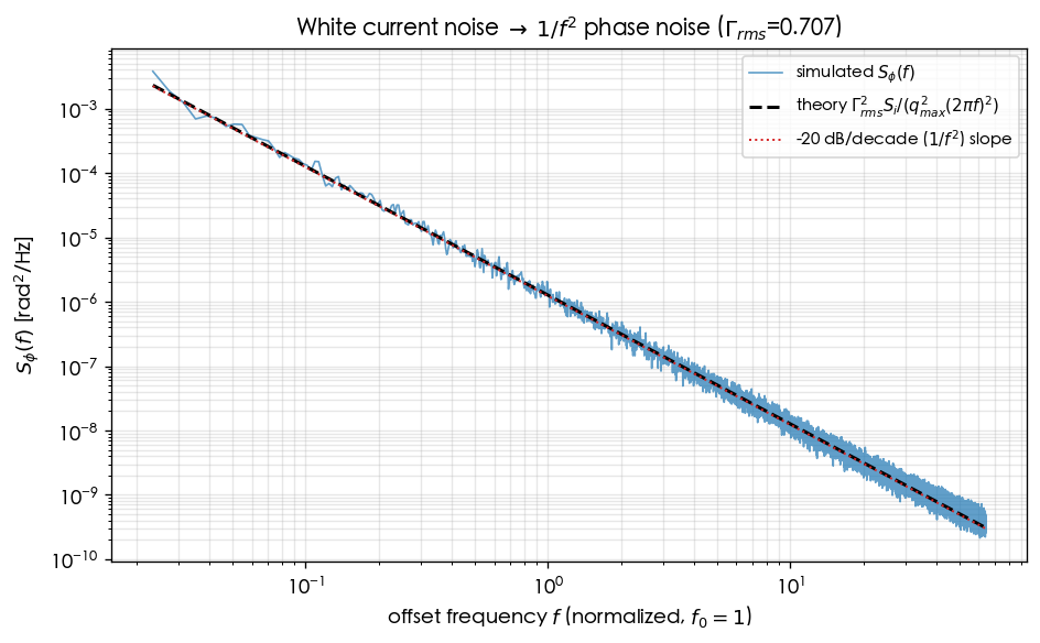
Figure 2: LC vs ring ISF shape and . lab_03's comparison figure: the ring's ISF sensitivity is concentrated at the transitions; the larger , the sharper each stage's ISF but the smaller its rms (). This explains where knob 3 in the scaling table comes from — and reminds you it is an isolated scaling.
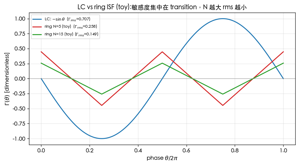
- How to use the two figures: Figure 1 tells you "the / knobs = a vertical shift"; Figure 2 tells you "how the ring's varies with ". Together they form the design map.
10. Corresponding paper equations/figures
- Main scaling: [P1] Eq.(21), p.185, .
- Parseval / : [P1] Eq.(20), p.185.
- Ring scaling: [P2] Eq.(16), p.794 (v7 re-verified: the square root covers only the constant, ; the body text's at η=0.75 and App. B Eq.(55) triple-confirm this. v3 had misread it as ).
- Ring frequency: [P2] Eq.(15), p.794, .
- Ring white-noise FOM: [P2] Eq.(23), p.796, ( is the stage-delay proportionality constant of [P2] Eq.(14), ; enters only through ).
- Concept figures: reuses
white_noise_phase_noise_psd.png(lab_06) andlc_vs_ring_isf_comparison.png(lab_03).
11. Limitations and approximations
- Toy scaling, not transistor-level: the scaling assumes "turn one knob, hold everything else exactly fixed". In a real circuit , , , power, area, and are coupled and cannot be tuned in isolation.
- Ring scaling ([P2] Eq.(16), p.794 — v7 re-verified: the square root covers only the constant, ; the body text's at η=0.75 and App. B Eq.(55) triple-confirm this. v3 had misread it as ): the proportionality constant is (); adding stages also changes , power, and area — the net phase noise/jitter requires the full FOM, not alone.
- Single white source: ignores multiple sources, cyclostationarity (), and flicker upconversion (, see lab_07). The table does not apply in the close-in region.
- Factor-of-2: uses Eq.(21)'s denominator ; it differs from the time-domain version by the factor-of-2 SSB bookkeeping, which affects none of the scaling conclusions (all dB changes are relative).
- Jitter scaling: assumes a fixed integration range and a shape; if close-in dominates, jitter is set by and the lower integration limit and must be computed separately.
Key takeaways
- phase noise ; jitter .
- Doubling or halving → phase noise dB, jitter halved ().
- Ring in isolation: ( dB), but /power/area change simultaneously — a toy scaling.
- Baseline numbers: pC, , 5 GHz @ 1 MHz, → dBc/Hz.
Further reading
- design: power_and_qmax
- Symmetry cuts : symmetry_and_1overf
- SerDes clocking: serdes_clocking_connection
- Applied to design/theory: turning the , , scalings into a topology decision → lc_vs_ring
- Upstream simulations: lab_06_white_noise_phase_noise, lab_08_jitter_integration