β: This English translation is in beta — the Traditional-Chinese original is the authoritative version.
A General Theory of Phase Noise in Electrical Oscillators
Prerequisites (recommended reading order): oscillator_phase (the geometry of the limit cycle and excess phase) → lti_vs_ltv (why an oscillator is LTV, not LTI) → stochastic_noise_basics (white/flicker noise PSD). This page is the foundation of the entire site — the other four deep dives all build on it.
This is the foundation of the whole course. It is the first work to model an oscillator's response to noise correctly as an LTV (linear time-variant) system, introducing the ISF (Impulse Sensitivity Function) and using it to derive, in one stroke, closed-form expressions for 1/f² and 1/f³ phase noise together with three design rules still in use today. The remaining four papers ([P2][P3][P4]) all build on the concepts on this page.
Citation
[P1] A. Hajimiri and T. H. Lee, "A General Theory of Phase Noise in Electrical Oscillators," IEEE J. Solid-State Circuits, vol. 33, no. 2, pp. 179–194, Feb. 1998. (file
general.pdf, paper_001)
One-sentence contribution
An oscillator's response to noise is not LTI but LTV: the same noise impulse injected at different phases of the waveform produces different phase shifts; this "phase sensitivity" is the ISF . With it, arbitrary noise can be propagated into phase noise, yielding the design rule (claim C1, C3).
Why this paper matters
Before [P1], engineering practice relied mainly on the Leeson model (1966, semi-empirical) — it draws the 1/f³, 1/f², and flat slope regions, but cannot explain why the 1/f³ corner does not equal the device's 1/f corner, or why some waveforms upconvert less flicker noise into close-in phase noise. [P1] supplies the physical answers:
- LTV, not LTI (claim C1): an oscillator is an autonomous system with no absolute time reference. A noise impulse landing on the waveform peak changes almost only the amplitude; one landing at a zero crossing converts almost entirely into phase. So "same impulse, different injection instant, different effect" — that is time variance. The LTI convolution cannot capture it.
- Phase accumulates permanently, amplitude is pulled back (claim C2): an oscillator has an amplitude-restoring mechanism that pulls amplitude perturbations back onto the limit cycle, but phase has no restoring force — every kick is kept forever. Phase noise lives in this accumulating phase.
- Quantify both points in a single function : phase noise is no longer fitted — it can be computed from the waveform and the noise PSD, and the computation points at the design knobs.
It also subsumes Leeson and cyclostationary noise as its own special cases (claim C9).
Main assumptions
Per paper_metadata (paper_001.assumptions):
- Noise is a small perturbation — the phase response can be linearized (requires ).
- Amplitude perturbations decay (stable limit cycle); only phase persists, so "tracking phase alone" suffices.
- The ISF is known, periodic, and frequency-independent — is a -periodic function determined solely by the steady-state waveform.
- Hard-switching / large-signal cyclostationary operation defines the ISF — is the sensitivity measured on that steady-state trajectory.
Physical intuition: draw the oscillator state in a 2-D plane; the steady state circulates along the limit cycle. A current impulse nudges the state point; the tangential component along the cycle becomes phase (kept forever), the radial component off the cycle becomes amplitude (pulled back). The same impulse kicked at different phases splits differently between tangential and radial — collect that ratio into a periodic function of the injection phase alone, and you have the ISF. Full geometry in oscillator_phase.
Key equations
Below are the most critical equations of [P1] (Eq.(1) and Eq.(9)–(24)). The LaTeX of each is
taken verbatim from Section 3 of the specification, with [P1] Eq.(n) page citations;
constants are never altered.
Eq.(1): output decomposition (where phase noise lives)
Original formula ([P1] Eq.(1), p.181):
Meaning: any oscillator output can be decomposed into an "instantaneous amplitude " times "the periodic waveform evaluated at ". is the steady-state waveform (not necessarily a sinusoid). Phase noise lives in the excess phase ; amplitude noise lives in .
Step-by-step: the ideal oscillation is ; once noise enters, the amplitude is perturbed into and the phase gains . Because amplitude has a restoring force (assumption 2), , so for phase-noise analysis can be treated as a constant and only tracked. This step collapses the problem from a "2-D state" to a "1-D phase".
Eq.(9): charge → voltage step (the physical entry point of noise)
Original formula ([P1] Eq.(9), p.182):
Meaning: a current impulse deposits charge on the node capacitance, instantly stepping the node voltage by . This is the physical entry point through which noise enters the oscillator state.
Dimension check: ✓.
Eq.(10)–(11): the ISF and the LTV phase response (the core)
Original formula ([P1] Eq.(10), p.182, excess-phase impulse response):
Original formula ([P1] Eq.(11), p.182, convolution form):
Meaning: is the dimensionless, -periodic ISF; is the maximum charge swing on the node. The (unit step) is crucial: once a phase step is created it persists forever (phase has no restoring force), so the impulse response carries a step rather than a decaying term. Eq.(11) is the superposition integral over all past noise.
Step-by-step derivation (no skipped steps):
Why is dimensionless: is in rad (dimensionless) and is also dimensionless, so must be dimensionless ✓. Note that depends on the absolute injection instant (through ), not merely on — exactly the fingerprint of an LTV system (claim C1). The full step-by-step derivations are in impulse_to_phase_shift and convolution_derivation.
Numerical example (Example A): pC, fC, , GHz.
Python verification:
from simulations.common.isf_utils import impulse_to_phase_step
from simulations.common.noise_utils import phase_to_time_error

dphi = impulse_to_phase_step(delta_q=1e-15, gamma_value=0.5, qmax=1e-12)
dt   = phase_to_time_error(dphi, f0=5e9)
print(dphi, "rad", dt*1e15, "fs")   # -> 0.0005 rad  15.92 fs
Eq.(12)–(13): Fourier series of the ISF and its harmonics
Original formula ([P1] Eq.(12), p.183):
Original formula ([P1] Eq.(13), p.183):
Meaning: expand the ISF in a Fourier series; each harmonic coefficient tells you "how strongly the oscillator moves noise near onto the carrier". (the DC term — the DC value of the ISF is ) is especially important — it is the only channel that upconverts the device's low-frequency 1/f noise into close-in 1/f³ phase noise (see Eq.(23)–(24)).
Step-by-step: substitute Eq.(12) into Eq.(11) and expand term by term to get Eq.(13). Physically this is a frequency-translation map ([P1] Fig. 8): noise near is down-converted by the -th harmonic into slow phase modulation at baseband. The full derivation and the notation trap ( vs ) are in fourier_series_of_isf.
Eq.(20): Parseval / rms ISF
Original formula ([P1] Eq.(20), p.185):
Meaning: summing the energy of all harmonics (Parseval) gives . This is what lets the "sum over all harmonics" of Eq.(19) collapse into a single clean .
Step-by-step: square both sides of Eq.(12), integrate over one period , and use trigonometric orthogonality (cross terms between different harmonics integrate to 0). Details in rms_isf.
Eq.(21): 1/f² phase noise (the signature result)
Original formula ([P1] Eq.(21), p.185):
Meaning: the SSB phase noise produced by a white-noise current source, in the 1/f² region ( dB/dec). Phase noise is proportional to (claim C3) — the most important of the three design rules: enlarge , shrink .
Step-by-step: from Eq.(16)/(17) obtain the phase modulation for a single injected tone (), from Eq.(18) the single-sideband power, then sum over all harmonics for white noise (Eq.(19)) and use Eq.(20) to collapse the sum into .
Numerical example (Example B): GHz, MHz, pC, , A²/Hz. rad/s, .
This is the ideal value for a single white-noise source; a real circuit has multiple sources, cyclostationarity, and flicker, so it sits higher. The full step-by-step account, including the famous factor-of-2 (SSB bookkeeping convention) discussion, is in white_noise_to_phase_noise.
Eq.(22)–(24): flicker upconversion and the 1/f³ corner
Original formula ([P1] Eq.(22), p.185, device flicker):
Original formula ([P1] Eq.(23), p.185, 1/f³ phase noise):
Original formula ([P1] Eq.(24), p.185, 1/f³ corner):
Meaning: the device's 1/f noise can be upconverted into close-in 1/f³ phase noise only through the DC term of the ISF (claim C4). The most counter-intuitive and most important point (claim C5): the 1/f³ corner the device 1/f corner — it is scaled by . If the waveform is symmetric and is small, the 1/f³ corner can be pushed far below . This is the mathematical basis of the "symmetry design rule".
Step-by-step: substitute the 1/f noise of Eq.(22) into Eq.(19); because only the DC coefficient has a DC response at baseband, only the term survives the sum, giving Eq.(23) (note the denominator is , not ). Setting the 1/f² of Eq.(21) equal to the 1/f³ of Eq.(23) and solving for the crossover frequency gives Eq.(24). The approximation comes from "a symmetric waveform is dominated by , so " (i.e. , hence , consistent with ).
Numerical example: if MHz and the waveform is symmetric enough that , then , i.e. a 1/f³ corner of kHz — far below the device's 1 MHz corner. Symmetry has pushed the close-in noise away by a factor of 200 in frequency. Full derivation in flicker_noise_upconversion.
Key figures
| Paper figure | Page | Content | Site counterpart |
|---|---|---|---|
| Fig. 4 | 181 | State-space effect of an impulse at the peak vs at a zero crossing | toy reproduction in lab_01/lab_02; see limit_cycle_phase_amplitude.png |
| Fig. 6 | 182 | Colpitts and 5-stage ring: excess phase vs injected charge (linear for small charge) | supports the linearity assumption |
| Fig. 7 | 183 | Waveforms and ISFs of (a) LC and (b) ring | toy counterpart lc_vs_ring_isf_comparison.png |
| Fig. 8 | 183 | Frequency-translation map: noise near moved onto the carrier | fourier_series_of_isf |
| Fig. 12 | 185 | and : 1/f³, 1/f², floor | flicker upconversion lab |
| Fig. 20–22 | 189–190 | Injection experiments: sideband , dB/dec, symmetric vs asymmetric node | see the Sec. V section below |
| Fig. 23–24 | 190–191 | Measured of the 232/115 MHz rings (distinct 1/f³ and 1/f² regions) | see the Sec. V section below |
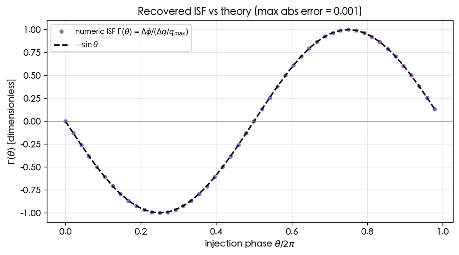
This site redraws the conceptual comparison with a Python toy model (not transistor-level):
Design insights
[P1] distills phase-noise design into three knobs (all read directly off Eq.(21) and Eq.(24)):
- Enlarge (node charge swing): ; every doubling of buys 6 dB. Larger capacitance, larger voltage swing, and higher power all push this way.
- Shrink : make the noise injection instants land where the ISF is small. The LC's is zero at the waveform peak, so "replenishing energy near the peak" hurts phase noise the least.
- Use symmetry to suppress : a waveform with symmetric rise/fall has , pushing the 1/f³ corner (Eq.(24)) very low and cutting close-in phase noise sharply. This rule is directly verified in the ring experiment of [P2] (Fig. 17).
Design-side summaries in symmetry and lc_vs_ring.
The paper's own end-to-end silicon validation (Sec. V)
What this section answers: this site's numeric chain (Example B's dBc/Hz) uses clean pedagogical numbers; the very same "process data → → → → → Eq.(21) → " pipeline was validated by [P1] Sec. V (pp.189–191) on real silicon with eight experiments, with prediction–measurement gaps of 0.2–0.7 dB — and every input is available a priori (process parameters, geometry, swing, extracted ISF); nothing is fitted after the fact. Below we first survey the eight experiments, then replay the chain with the most complete numbers step by step.
The eight experiments at a glance (numbers transcribed verbatim from [P1] pp.189–191):
| # | Experiment | What it verifies | Paper's result |
|---|---|---|---|
| 1 | 5-stage 5.4 MHz CMOS ring, sinusoidal current injection, sweeping amplitude ( kHz, MHz, MHz, MHz) | Linearity of current→sideband in Eq.(18) | Upper/lower sidebands equal (within the 0.2 dB accuracy of the setup); best-fit slope 19.8 dB/decade vs predicted 20 (Fig. 20) |
| 2 | Same ring, 20 µA (rms), sweeping | The dependence of Eq.(18) | All four injection frequencies give dB/decade (Fig. 21) |
| 3 | 5-stage ring, one stage made asymmetric with an extra pulldown NMOS, 20 µA (rms) injected | Low-frequency upconversion is set by (waveform symmetry) | Sidebands 7 dB larger at the asymmetric node; symmetric nodes essentially unchanged (Fig. 22) |
| 4 | 5-stage 232 MHz single-ended ring (2-µm, 5-V CMOS) | The full Eq.(21) + Eq.(24) chain | Predicted vs measured dBc/Hz @ 500 kHz; corner predicted 75 vs measured 80 kHz (Fig. 23) |
| 5 | 11-stage 115 MHz ring (same die) | Same chain with different and device sizes | Predicted vs measured dBc/Hz @ 500 kHz; corner predicted 43 vs measured 45 kHz (Fig. 24) |
| 6 | 7-stage current-starved ring ( held at 60/50 MHz), control voltages tune rise/fall independently | Symmetry should move only 1/f³, not 1/f² (Eq.(24), Eq.(30)) | Tuning symmetry strongly suppresses the 1/f³ region while barely touching 1/f²; an optimum symmetry point exists (Fig. 25/26) |
| 7 | 4-stage differential 200 MHz ring (0.5-µm) | Eq.(21); "only half-circuit symmetry counts" | Predicted vs measured dBc/Hz @ 1 MHz; a distinct 1/f³ region despite differential symmetry (Fig. 27) |
| 8 | Bipolar Colpitts 100 MHz, sweeping ( fixed) | Conduction-angle effect of cyclostationary noise / | A definite optimum conduction angle exists; phase noise minimized near — the theoretical basis for the classic Colpitts rule of thumb (Fig. 28) |
Full-chain replay: the fourth experiment (5-stage, 232 MHz, 2-µm 5-V CMOS)
This is the chain with the most complete numbers in the whole paper — every input is printed on p.190, and we substitute them back step by step.
Step 0 — the paper's process/geometry inputs ([P1] p.190, transcribed verbatim):
| Quantity | Value | Unit |
|---|---|---|
| gate oxide thickness | 25 | nm |
| 0.6 | V | |
| 0.53 | V | |
| 3 µm / 2 µm | — | |
| 5 µm / 2 µm | — | |
| lateral diffusion | 0.1 | µm (so µm) |
| total node capacitance (incl. parasitics, computed from process + geometry) | 35.7 | fF |
| measurement method | delay-based | — (Fig. 23 shows distinct 1/f³ and 1/f² regions) |
Step 1 — : 5-V process, node swing V:
The paper rounds this to 179 fC. Dimension check: F × V = C ✓ (fF × V = fC).
Step 2 — noise PSD at the transition point: a ring's (effective) ISF is concentrated at the transitions (this site's lc_vs_ring and [P2]), so the paper evaluates the noise only at "the instant the output crosses "; at that point the NMOS and PMOS are simultaneously on, and their current-noise powers add (p.190):
(This is channel thermal noise in the form with the bias point taken at ; the paper does not list the individual values of and — the two PSDs above are given directly by the paper.) Per stage, the total is:
(Numeric feel: this site's canonical A²/Hz is the same order of magnitude as this 2-µm real-silicon .)
Step 3 — : using the methods of the Appendix, the paper obtains, for rings,
(Dimensionless ✓.) This is the direct ancestor of [P2] Eq.(16): , which with gives — the 1998 and 1999 papers mesh with each other. Incidentally , the same order as this site's representative 0.5 and smaller than the true-LC .
Step 4 — substitute into Eq.(21) ( identical, uncorrelated sources): the powers of uncorrelated sources add, A²/Hz:
The numerator is and the denominator is , so
which matches the printed on p.190 of the paper (our recomputation gives 0.839). Dimension check: the unit of is , and dividing by the Hz² of gives 1/Hz — exactly the dimension of "sideband power per Hz relative to the carrier" ✓. (In other words the prefactor 0.84 carries the unit Hz.)
Step 5 — prediction vs measurement: substituting kHz:
The paper measures dBc/Hz — a 0.2 dB gap.
factor-of-2/4 flag (called out every time it appears): the 4 in the denominator is [P1] Eq.(21)'s SSB bookkeeping, the same convention as this site's Example B ( dBc/Hz). With the clean time-domain /2 bookkeeping instead, the same inputs would predict dBc/Hz (3 dB higher), i.e. 3.0 dB away from the measurement. This experiment is therefore often cited as empirical support for the /4 version; note, however, that the 0.2 dB agreement also absorbs estimation errors in and , so reading it as "the magnitude and scaling are right" is more robust than reading it as a definitive verdict on the factor of 2. See white_noise_to_phase_noise.
Step 6 — the 1/f³ corner (Eq.(24) divided through by ): an isolated inverter on the same die (input and output shorted) measures a device 1/f corner of kHz; from the extracted ISF, :
Measured: 80 kHz. This is the most direct silicon evidence for claim C5, "the 1/f³ corner the device 1/f corner": the corner is pushed from 250 kHz down to 80 kHz by the (partial) symmetry of the waveform.
Python verification (pure-algebra recomputation; all inputs from [P1] p.190–191):
import math

# [P1] Sec. V, fourth experiment: 5-stage 232 MHz single-ended ring (2-µm 5-V CMOS, p.190)
N       = 5              # number of stages
qmax    = 179e-15        # C (= C_total 35.7 fF × V_swing 5 V)
Si_nmos = 4.44e-24       # A²/Hz (given by the paper, p.190, at the transition point)
Si_pmos = 2.19e-24       # A²/Hz (given by the paper, p.190)
G2rms   = 16 / N**3      # Γ²_rms ≈ 16/N³ (paper, p.190)

print(round(G2rms, 3))                            # -> 0.128
Si_total = N * (Si_nmos + Si_pmos)                # powers of N uncorrelated sources add
prefac = G2rms * Si_total / (4 * qmax**2 * (2*math.pi)**2)
print(round(prefac, 3))                           # -> 0.839 (paper prints 0.84)

df = 500e3   # Hz
print(round(10*math.log10(prefac/df**2), 2))      # -> -114.74 (paper predicts -114.7; measured -114.5)
print(round(10*math.log10(2*prefac/df**2), 2))    # -> -111.73 (with the time-domain /2 bookkeeping: 3 dB off the measurement)
print(round(250e3*0.3/1e3, 1))                    # -> 75.0 (kHz, Eq.(24); measured 80 kHz)

# Fifth experiment: 11-stage 115 MHz (same die; noise scales with W: NMOS×4/3, PMOS×6/5, same L)
N2, qmax2 = 11, 217e-15
Si_stage2 = Si_nmos*(4/3) + Si_pmos*(6/5)
prefac2 = (16/N2**3) * N2 * Si_stage2 / (4 * qmax2**2 * (2*math.pi)**2)
print(round(prefac2, 3))                          # -> 0.152 (paper prints 0.152, digit-for-digit)
print(round(10*math.log10(prefac2/df**2), 2))     # -> -122.16 (paper predicts -122.1; measured -122.5)
print(round(250e3*0.17/1e3, 1))                   # -> 42.5 (kHz, paper rounds to 43; measured 45 kHz)

# Seventh experiment: 4-stage differential 200 MHz (0.5-µm; q_max = 49 fF × 1.2 V = 58.8 fC)
prefac3 = (16/4**3) * 4 * 2.63e-23 / (4 * (58.8e-15)**2 * (2*math.pi)**2)
print(round(prefac3, 1))                          # -> 48.2 (paper prints 48.1, trailing-digit rounding)
print(round(10*math.log10(prefac3/(1e6)**2), 2))  # -> -103.17 (paper predicts -103.2; measured -103.9)
Second validation on the same die: the 11-stage 115 MHz ring
The fifth experiment reruns the same chain with different and device sizes ([P1] p.190, numbers verbatim): µm / 2 µm, µm / 2 µm, total node capacitance 43.5 fF, fC (). The paper states the phase noise is "calculated in exactly the same manner as the previous experiment", giving , i.e. dBc/Hz at 500 kHz; measured dBc/Hz (0.4 dB gap). predicts a 1/f³ corner of 43 kHz; measured 45 kHz. The paper does not list the device PSDs of the 11-stage inverters; the Python above recomputes them by scaling the noise linearly with (same ) and lands on a prefactor of 0.152, digit-for-digit identical to the paper — reverse-confirming that this is exactly the paper's internal calculation.
As a bonus, we can itemize the 7.4 dB improvement from 5 stages to 11 stages entirely inside Eq.(21) (using the two recomputed prefactors, dB):
| Term | Ratio | dB |
|---|---|---|
| () | smaller | |
| ( fC) | larger | |
| per-stage noise PSD ( A²/Hz) | larger | |
| Total | ✓ |
Note this is not a free lunch: the stage count grows and also drops from 232 to 115 MHz; [P2] Eq.(23), p.796 later proves that at fixed total power and fixed the white-noise phase noise of a single-ended ring is independent of . See paper_002.
Third validation across process and architecture: 4-stage differential 200 MHz (0.5-µm)
The seventh experiment ([P1] p.191): tail current 108 µA, total capacitance on each differential node fF, V, hence fC (the paper's text prints "58.8 fF" — dimensionally can only be fC; this is a typo in the paper, which we transcribe faithfully and flag). Total channel noise per node A²/Hz; with the same chain gives (our recomputation gives 48.2, a trailing-digit rounding difference), predicting at 1 MHz; measured dBc/Hz (0.7 dB gap).
The same experiment carries a symmetry lesson: although the differential signal is perfectly symmetric, the single-ended waveform of each half-circuit is not, so Fig. 27 still shows a distinct 1/f³ region — "differential signaling does not rescue ; what counts is half-circuit symmetry" (echoing p.188 and symmetry).
What this set of experiments establishes (applicability and failure conditions)
- The predictions are a priori: the three full chains (232 MHz / 115 MHz / 200 MHz differential) miss by 0.2 / 0.4 / 0.7 dB, with inputs limited to process parameters, geometry, , and the extracted ISF. This site's Example B toy chain ( pC, , A²/Hz → dBc/Hz @ 1 MHz, SSB /4 bookkeeping) runs the very same pipeline, just with clean numbers.
- Applicable when: noise is concentrated at the transitions (true for single-ended CMOS rings); is a ring-specific approximation for "identical inverters with standard rise/fall" (corresponding to [P2]'s ); the noise of different stages is uncorrelated (only then may powers be added).
- Fails when: the waveform is asymmetric (experiments 3/6/7) so that close-in noise is dominated by the -driven 1/f³ — Eq.(21) covers only the 1/f² region; very close to the carrier the linearization breaks down (see lorentzian_linewidth); strong spurs or injection pulling require separate treatment ([P3]/[P4]).
- Dimensions: the argument of every is 1/Hz — the hallmark of dBc/Hz.
Limitations
Per paper_metadata (paper_001.limitations):
- The 1/f³ region was historically linked empirically; this theory clarifies that it is set by , but the exact still has to be extracted.
- In real circuits must be extracted via transient impulse simulation or adjoint/PSS methods; the closed forms are first-order approximations.
- AM–PM conversion and strong nonlinearity are not fully covered by the first-order phase-only model (exactly the hole [P4] patches with the APF).
- The rigorous mathematical foundation (PPV / adjoint / Floquet) is not among the five source PDFs; it belongs to external literature (claim C13) — see effective_isf.
Relationship to other papers
- [P2] applies this page's ISF to the ring oscillator: it derives the jitter from the same ratio and studies the scaling (claim C8).
- [P3]/[P4] extend the same ISF from "random noise" to "deterministic injection": [P3] uses to write the generalized Adler equation (claim C10); [P4] adds the amplitude counterpart, the APF (claim C11).
- [P5] is unrelated to this page (sense amplifier, claim C12); the only conceptual bridge is regeneration / positive feedback.
- The Leeson model is a special case of this theory (claim C9); the Leeson formula is entry 19 in equation_index, marked as reference (not in the 5 PDFs).
Further reading / companion teaching pages
This page is the bird's-eye view "at the altitude of the paper"; the five pages below take each block of [P1] all the way through, step by step. Recommended order:
| Which block of this page | Companion teaching page | What that page adds |
|---|---|---|
| Eq.(10)–(13) ISF and LTV phase response | isf_definition | The full definition of the ISF; its periodicity and dimensionlessness built up term by term |
| Eq.(11) convolution form | convolution_derivation | From the impulse response to the superposition integral with no skipped steps, incl. the LTV fingerprint |
| Eq.(19)–(21) white noise 1/f² phase noise | white_noise_to_phase_noise | downconversion, the factor-8 summation, the famous factor-of-2 SSB bookkeeping controversy |
| Eq.(22)–(24) flicker upconversion and the 1/f³ corner | flicker_noise_upconversion | why only can upconvert; the complete algebra behind 1/f³ corner device corner |
| "Use symmetry to suppress " among the three design rules | symmetry | how symmetry sets , the design knobs, and the experimental cross-check with [P2] Fig. 17 |
How to read: the theory details and numerical feel all live in 03_isf_core_theory; to compute hands-on, go back to numerical_feeling. This page's only job is to string those blocks into the story of one paper.
What to remember
- LTV, not LTI: same impulse, different injection phase, different effect — that is the ISF .
- Phase accumulates, amplitude is pulled back: phase noise lives in the accumulating phase (Eq.(1); the upper limit of the integral in Eq.(11) is ).
- Signature formula: (Eq.(21)).
- Three design rules: enlarge , shrink , use symmetry to suppress .
- 1/f³ corner device 1/f corner (Eq.(24)) — symmetry can push it very low.
- All core derivations are in 03_isf_core_theory; numerical feel is in numerical_feeling.